Ro
-
 KAIST to Host the 2017 AI World Cup in November
KAIST, the birthplace of the Robot World Cup in 1996, now presents a new technology matchup, the AI World Cup this November, which will be held at KAIST. The event is being organized by the Machine Intelligence and Robotics Multi-Sponsored Research and Education Platform (MIR-MSREP) of KAIST. The online, simulated AI soccer game, based on rolling updates, will be a draw for avid online gamers and tech-savvy university students from around the nation.
The tournament is comprised of three events: ▲A 5 on 5 AI soccer match to be played after self-learning using AI technology in an online simulation environment ▲Commentary in which online soccer videos are analyzed and commented on, and ▲Game reporters who will write articles on online soccer event results.
The participants will undergo a month-long online practice period in October and compete in preliminary matches from November 1 through 24. The top teams that scored the highest accumulated points will compete in the finals on December 1. In the finals, each team’s AI technology implementation method will be evaluated to select the final winning team. To ensure a successful event, KAIST will host a briefing session for participants on July 28.
Technological prowess and early exposure to AI accumulated at KAIST led to the launching of this tournament. Professor Jong-Hwan Kim, the chair of the Organizing Committee of the AI World Cup, hosted the first ever Robot World Cup back in 1996. His concept has now evolved into the emerging technology of AI and the members of the Organizing Committee encompass the professors from the various departments of electrical engineering, computing, industrial and systems engineering, aerospace engineering, civil and environmental engineering, and the graduate schools of Green Transportation, Cultural Technology, and Science and Technology Policy.
In particular, ongoing convergence research initiatives incorporating AI into a wide arrays of disciplines such as bio, nano, and IT, played a crucial role for making this AI World Cup happen. Professor Kim said, “The winner of this year’s competition will be awarded a certificate and a small gift. In 2018, we aim to expand the event to an international scale by allowing international teams.”
Any undergraduate or graduate student in Korea can apply to participate in the ‘AI World Cup 2017’. KAIST will host a public trial event during the ‘Open KAIST’ event period to be held November 2-3 to help participating students understand the event better. ‘Open KAIST’ allows the general public to personally visit and experience what goes on in engineering departments and laboratories on the KAIST main campus. It is hosted by the College of Engineering every two years and is the largest event hosted by KAIST.
To participate in the ‘AI World Cup 2017,’ teams consisting of Korean undergraduates or graduate students can fill out application forms and submit them by September 30 on http://mir.kaist.ac.kr .
2017.07.14 View 13842
KAIST to Host the 2017 AI World Cup in November
KAIST, the birthplace of the Robot World Cup in 1996, now presents a new technology matchup, the AI World Cup this November, which will be held at KAIST. The event is being organized by the Machine Intelligence and Robotics Multi-Sponsored Research and Education Platform (MIR-MSREP) of KAIST. The online, simulated AI soccer game, based on rolling updates, will be a draw for avid online gamers and tech-savvy university students from around the nation.
The tournament is comprised of three events: ▲A 5 on 5 AI soccer match to be played after self-learning using AI technology in an online simulation environment ▲Commentary in which online soccer videos are analyzed and commented on, and ▲Game reporters who will write articles on online soccer event results.
The participants will undergo a month-long online practice period in October and compete in preliminary matches from November 1 through 24. The top teams that scored the highest accumulated points will compete in the finals on December 1. In the finals, each team’s AI technology implementation method will be evaluated to select the final winning team. To ensure a successful event, KAIST will host a briefing session for participants on July 28.
Technological prowess and early exposure to AI accumulated at KAIST led to the launching of this tournament. Professor Jong-Hwan Kim, the chair of the Organizing Committee of the AI World Cup, hosted the first ever Robot World Cup back in 1996. His concept has now evolved into the emerging technology of AI and the members of the Organizing Committee encompass the professors from the various departments of electrical engineering, computing, industrial and systems engineering, aerospace engineering, civil and environmental engineering, and the graduate schools of Green Transportation, Cultural Technology, and Science and Technology Policy.
In particular, ongoing convergence research initiatives incorporating AI into a wide arrays of disciplines such as bio, nano, and IT, played a crucial role for making this AI World Cup happen. Professor Kim said, “The winner of this year’s competition will be awarded a certificate and a small gift. In 2018, we aim to expand the event to an international scale by allowing international teams.”
Any undergraduate or graduate student in Korea can apply to participate in the ‘AI World Cup 2017’. KAIST will host a public trial event during the ‘Open KAIST’ event period to be held November 2-3 to help participating students understand the event better. ‘Open KAIST’ allows the general public to personally visit and experience what goes on in engineering departments and laboratories on the KAIST main campus. It is hosted by the College of Engineering every two years and is the largest event hosted by KAIST.
To participate in the ‘AI World Cup 2017,’ teams consisting of Korean undergraduates or graduate students can fill out application forms and submit them by September 30 on http://mir.kaist.ac.kr .
2017.07.14 View 13842 -
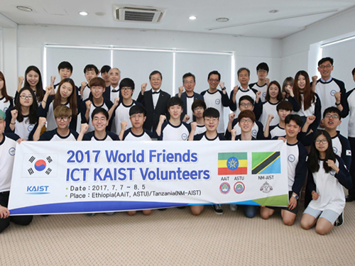 2017 World Friends ICT KAIST Sets Off to Ethiopia, Tanzania
KAIST launched the ‘2017 World Friends ICT KAIST’ on 21 June at a ceremony held at the Faculty Club. The event was attended by 40 student volunteers and faculty members including President Sung-Chul Shin and student volunteers.
The ‘2017 World Friends ICT KAIST’ is an oversees volunteer program aimed at providing ICT education for students from developing countries and for cultural exchange. The program was organized by the KAIST Leadership Center and sponsored by the National Information Agency (NIA) since 2015.
President Sung-Chul Shin delivered words of encouragement to start the opening ceremony, followed by an oath-taking by the volunteer group, safety training, and a commemorative photoshoot. This year’s World Friends ICT volunteer group consisted of 32 students and 2 staff members to lead and to support the team.
The group was divided into eight teams including APP-frica, KAI-Tigers, and WITH (4 members per team) to volunteer in Addis Ababa Institute of Technology (AAIT) and Adama Science and Technology University in Ethiopia (ASTU), as well as Nelson Mandela African Institute of Science and Technology (NM-AIST) in Tanzania. The teams will educate local students on ICT and promote cultural exchanges. The volunteer period is from July 7 to August 5, lasting about a month.
KAIST conducted primary document examinations and interviews from April 27 to May 18 on volunteer candidates who registered to take part, and selected 32 student volunteers. A total of 68 students registered to volunteer, resulting in a 1:2.1 competition rate.
The volunteering program was customized to the local needs of Ethiopia and Tanzania and thus consisted of ICT education, cultural exchanges, volunteering at farms on the weekends, and science experiments. The area with the most focus by the volunteer team is ICT education, which accounts for 70% of the total volunteer activities. The aim is to educate Ethiopian students at AAIT and ASTU on Windows, MS Office, Adobe Photoshop, and using smartphones. In Tanzania, the team is to volunteer with students of NM-AIST to provide ICT application education such as water tank control using appropriate technology and Arduino to local high school students.
The team is also planning to promote cultural exchanges by preparing K-Pop dancing, traditional Korean games such as Korean shuttlecock game (jegichagi) and Korean wrestling (ssireum), traditional cooking such as bibimbab and half-moon-shaped rice cake (songpyeon), and teaching the Korean language, as well as preparing cultural performances with local university students. On the weekends, the team will visit local farms to volunteer, and local elementary schools and orphanages to conduct science experiments for children, as well as physical education and art activities.
(Photo caption: Volunteers poses with faculty and staff members including President Sung-Chul Shin at a ceremony on June 21.)
2017.06.29 View 13220
2017 World Friends ICT KAIST Sets Off to Ethiopia, Tanzania
KAIST launched the ‘2017 World Friends ICT KAIST’ on 21 June at a ceremony held at the Faculty Club. The event was attended by 40 student volunteers and faculty members including President Sung-Chul Shin and student volunteers.
The ‘2017 World Friends ICT KAIST’ is an oversees volunteer program aimed at providing ICT education for students from developing countries and for cultural exchange. The program was organized by the KAIST Leadership Center and sponsored by the National Information Agency (NIA) since 2015.
President Sung-Chul Shin delivered words of encouragement to start the opening ceremony, followed by an oath-taking by the volunteer group, safety training, and a commemorative photoshoot. This year’s World Friends ICT volunteer group consisted of 32 students and 2 staff members to lead and to support the team.
The group was divided into eight teams including APP-frica, KAI-Tigers, and WITH (4 members per team) to volunteer in Addis Ababa Institute of Technology (AAIT) and Adama Science and Technology University in Ethiopia (ASTU), as well as Nelson Mandela African Institute of Science and Technology (NM-AIST) in Tanzania. The teams will educate local students on ICT and promote cultural exchanges. The volunteer period is from July 7 to August 5, lasting about a month.
KAIST conducted primary document examinations and interviews from April 27 to May 18 on volunteer candidates who registered to take part, and selected 32 student volunteers. A total of 68 students registered to volunteer, resulting in a 1:2.1 competition rate.
The volunteering program was customized to the local needs of Ethiopia and Tanzania and thus consisted of ICT education, cultural exchanges, volunteering at farms on the weekends, and science experiments. The area with the most focus by the volunteer team is ICT education, which accounts for 70% of the total volunteer activities. The aim is to educate Ethiopian students at AAIT and ASTU on Windows, MS Office, Adobe Photoshop, and using smartphones. In Tanzania, the team is to volunteer with students of NM-AIST to provide ICT application education such as water tank control using appropriate technology and Arduino to local high school students.
The team is also planning to promote cultural exchanges by preparing K-Pop dancing, traditional Korean games such as Korean shuttlecock game (jegichagi) and Korean wrestling (ssireum), traditional cooking such as bibimbab and half-moon-shaped rice cake (songpyeon), and teaching the Korean language, as well as preparing cultural performances with local university students. On the weekends, the team will visit local farms to volunteer, and local elementary schools and orphanages to conduct science experiments for children, as well as physical education and art activities.
(Photo caption: Volunteers poses with faculty and staff members including President Sung-Chul Shin at a ceremony on June 21.)
2017.06.29 View 13220 -
 Observation of the Phase Transition of Liquid Crystal Defects
KAIST researchers observed the phase transition of topological defects formed by liquid crystal (LC) materials for the first time.
The phase transition of topological defects, which was also the theme of the Nobel Prize for Physics in 2016, can be difficult to understand for a layperson but it needs to be studied to understand the mysteries of the universe or the underlying physics of skyrmions, which have intrinsic topological defects.
If the galaxy is taken as an example in the universe, it is difficult to observe the topological defects because the system is too large to observe some changes over a limited period of time. In the case of defect structures formed by LC molecules, they are not only a suitable size to observe with an optical microscope, but also the time period in which the phase transition of a defect occurring can be directly observed over a few seconds, which can be extended to a few minutes. The defect structures formed by LC material have radial, circular, or spiral shapes centering on a singularity (defect core), like the singularity that was already introduced in the famous movie "Interstellar,” which is the center point of black hole.
In general, LC materials are mainly used in liquid crystal displays (LCDs) and optical sensors because it is easy to control their specific orientation and they have fast response characteristics and huge anisotropic optical properties. It is advantageous in terms of the performance of LCDs that the defects of the LC materials are minimized. The research team led by Professor Dong Ki Yoon in the Graduate School of Nanoscience and Technology did not simply minimize such defects but actively tried to use the LC defects as building blocks to make micro- and nanostructures for the patterning applications. During these efforts, they found the way to directly study the phase transition of topological defects under in-situ conditions.
Considering the LC material from the viewpoint of a device like a LCD, robustness is important. Therefore, the LC material is injected through the capillary phenomenon between a rigid two-glass plate and the orientation of the LCs can be followed by the surface anchoring condition of the glass substrate. However, in this conventional case, it is difficult to observe the phase transition of the LC defect due to this strong surface anchoring force induced by the solid substrate.
In order to solve this problem, the research team designed a platform, in which the movement of the LC molecules was not restricted, by forming a thin film of LC material on water, which is like oil floating on water. For this, a droplet of LC material was dripped onto water and spread to form a thin film. The topological defects formed under this circumstance could show the thermal phase transition when the temperature was changed. In addition, this approach can trace back the morphology of the original defect structure from the sequential changes during the temperature changes, which can give hints to the study of the formation of topological defects in the cosmos or skyrmions.
Prof. Yoon said, “The study of LC crystal defects itself has been extensively studied by physicists and mathematicians for about 100 years. However, this is the first time that we have observed the phase transition of LC defects directly.” He also added, "Korea is leading in the LCD industry, but our basic research on LCs is not at the world's research level."
The first author of this study is Dr. Min-Jun Gimand supported by a grant from the National Research Foundation (NRF) and funded by the Korean Government (MSIP). The research result was published on May 30, 2017 in Nature Communications.
Figure 1. The phase transition of the LC topological defect on cooling.
Figure 2. Polarizing optical microscopy images of topological defects depending on the strength of the director field. (a,b,e) Convergent director field arrangements of LC molecules and corresponding schematic images; (c,d,f) Divergent director field arrangements of LC molecules and corresponding schematic images.
2017.06.02 View 11546
Observation of the Phase Transition of Liquid Crystal Defects
KAIST researchers observed the phase transition of topological defects formed by liquid crystal (LC) materials for the first time.
The phase transition of topological defects, which was also the theme of the Nobel Prize for Physics in 2016, can be difficult to understand for a layperson but it needs to be studied to understand the mysteries of the universe or the underlying physics of skyrmions, which have intrinsic topological defects.
If the galaxy is taken as an example in the universe, it is difficult to observe the topological defects because the system is too large to observe some changes over a limited period of time. In the case of defect structures formed by LC molecules, they are not only a suitable size to observe with an optical microscope, but also the time period in which the phase transition of a defect occurring can be directly observed over a few seconds, which can be extended to a few minutes. The defect structures formed by LC material have radial, circular, or spiral shapes centering on a singularity (defect core), like the singularity that was already introduced in the famous movie "Interstellar,” which is the center point of black hole.
In general, LC materials are mainly used in liquid crystal displays (LCDs) and optical sensors because it is easy to control their specific orientation and they have fast response characteristics and huge anisotropic optical properties. It is advantageous in terms of the performance of LCDs that the defects of the LC materials are minimized. The research team led by Professor Dong Ki Yoon in the Graduate School of Nanoscience and Technology did not simply minimize such defects but actively tried to use the LC defects as building blocks to make micro- and nanostructures for the patterning applications. During these efforts, they found the way to directly study the phase transition of topological defects under in-situ conditions.
Considering the LC material from the viewpoint of a device like a LCD, robustness is important. Therefore, the LC material is injected through the capillary phenomenon between a rigid two-glass plate and the orientation of the LCs can be followed by the surface anchoring condition of the glass substrate. However, in this conventional case, it is difficult to observe the phase transition of the LC defect due to this strong surface anchoring force induced by the solid substrate.
In order to solve this problem, the research team designed a platform, in which the movement of the LC molecules was not restricted, by forming a thin film of LC material on water, which is like oil floating on water. For this, a droplet of LC material was dripped onto water and spread to form a thin film. The topological defects formed under this circumstance could show the thermal phase transition when the temperature was changed. In addition, this approach can trace back the morphology of the original defect structure from the sequential changes during the temperature changes, which can give hints to the study of the formation of topological defects in the cosmos or skyrmions.
Prof. Yoon said, “The study of LC crystal defects itself has been extensively studied by physicists and mathematicians for about 100 years. However, this is the first time that we have observed the phase transition of LC defects directly.” He also added, "Korea is leading in the LCD industry, but our basic research on LCs is not at the world's research level."
The first author of this study is Dr. Min-Jun Gimand supported by a grant from the National Research Foundation (NRF) and funded by the Korean Government (MSIP). The research result was published on May 30, 2017 in Nature Communications.
Figure 1. The phase transition of the LC topological defect on cooling.
Figure 2. Polarizing optical microscopy images of topological defects depending on the strength of the director field. (a,b,e) Convergent director field arrangements of LC molecules and corresponding schematic images; (c,d,f) Divergent director field arrangements of LC molecules and corresponding schematic images.
2017.06.02 View 11546 -
 KAIST Nanosatellite LINK Launched to the ISS
Courtesy: United Launch Alliance
The KAIST nanosatellite LINK (Little Intelligent Nanosatellite of KAIST) was successfully launched on an Atlas V booster aboard the NASA CRS-7 Mission on April 18 at Space Launch Complex 41, Cape Canaveral Air Force Station in Florida. The KAIST nanosatellite was developed by the research team led by Professor Hyochoong Bang of the Department of Aerospace Engineering.
Aboard the flight to the ISS (International Space Station) were 28 satellites including LINK. They are part of the QB50 Project, an international educational initiative which aims to deploy an array of CubeSat-mounted sensors into Earth’s thermosphere. The project is funded by the European Commission and managed by the von Karman Institute for Fluid Dynamics in Belgium.
The small satellites are hitching a lift into orbit aboard the unmanned resupply spacecraft Cygnus, with a total mass of 83 kilograms. Built to CubeSat specifications, Cygnus will deploy four of the spacecraft following its departure from the space station. LINK will conduct its scientific mission for three months at the station.
The majority of QB50 satellites carry one of three standard instrument packages, consisting of a primary instrument and an array of thermistors, thermocouples, and resistant temperature detectors. LINK is a two-unit CubeSat and weighs two kilograms. It carries an ion-neutral mass spectrometer (INMS), which measures the mass of ions and neutral atoms, as the primary payload of the QB50 project. The secondary payload is two Langmuir probes, which are in-house sensors (m-NLP) developed by Professor Kyong Wook Min’s team of the Department of Physics at KAIST. These are all geared toward collecting long-term continuous in-situ measurements of conditions in Earth’s lower thermosphere.
Professor Bang said, “The QB50 Project is being used for educational purposes. However, the LINK launch will bring a new breakthrough toward collecting information on Earth’s lower thermosphere. Building on these experiences of designing and launching the CubeSat will serve as an opportunity to verify the research results made in our lab firsthand in space.”
(Caption: LINK (Little Intelligent Nanosatellite of KAIST) was launched on an Atlast V booster aboard the NASA CRS-7 Mission on April 18.)
2017.04.25 View 9885
KAIST Nanosatellite LINK Launched to the ISS
Courtesy: United Launch Alliance
The KAIST nanosatellite LINK (Little Intelligent Nanosatellite of KAIST) was successfully launched on an Atlas V booster aboard the NASA CRS-7 Mission on April 18 at Space Launch Complex 41, Cape Canaveral Air Force Station in Florida. The KAIST nanosatellite was developed by the research team led by Professor Hyochoong Bang of the Department of Aerospace Engineering.
Aboard the flight to the ISS (International Space Station) were 28 satellites including LINK. They are part of the QB50 Project, an international educational initiative which aims to deploy an array of CubeSat-mounted sensors into Earth’s thermosphere. The project is funded by the European Commission and managed by the von Karman Institute for Fluid Dynamics in Belgium.
The small satellites are hitching a lift into orbit aboard the unmanned resupply spacecraft Cygnus, with a total mass of 83 kilograms. Built to CubeSat specifications, Cygnus will deploy four of the spacecraft following its departure from the space station. LINK will conduct its scientific mission for three months at the station.
The majority of QB50 satellites carry one of three standard instrument packages, consisting of a primary instrument and an array of thermistors, thermocouples, and resistant temperature detectors. LINK is a two-unit CubeSat and weighs two kilograms. It carries an ion-neutral mass spectrometer (INMS), which measures the mass of ions and neutral atoms, as the primary payload of the QB50 project. The secondary payload is two Langmuir probes, which are in-house sensors (m-NLP) developed by Professor Kyong Wook Min’s team of the Department of Physics at KAIST. These are all geared toward collecting long-term continuous in-situ measurements of conditions in Earth’s lower thermosphere.
Professor Bang said, “The QB50 Project is being used for educational purposes. However, the LINK launch will bring a new breakthrough toward collecting information on Earth’s lower thermosphere. Building on these experiences of designing and launching the CubeSat will serve as an opportunity to verify the research results made in our lab firsthand in space.”
(Caption: LINK (Little Intelligent Nanosatellite of KAIST) was launched on an Atlast V booster aboard the NASA CRS-7 Mission on April 18.)
2017.04.25 View 9885 -
 Expanding the Genetic Code of Mus Musculus
Professor Hee-Sung Park of the Department of Chemistry, who garnered attention for his novel strategy of installing authentic post-translational modifications into recombinant proteins, expanded his research portfolio to another level. Professor Park’s team was the first to report the generation of a mouse strain with an expanded genetic code, allowing site-specific incorporation of unnatural amino acids.
Professor Park published the research on the new chemical biology method for achieving selective chemical modifications in proteins in Science last September. The research team, this time in collaboration with Professor Chan Bae Park of the Department of Physiology at the Ajou University School of Medicine, demonstrated temporal and spatial control of protein acetylation in various organs of the transgenic mouse using a recombinant green fluorescent protein as a model protein. This research was published in the online edition of Nature Communications on February 21.
This approach enables the rapid onset of position-specific acetylation of a target protein at any developmental stage, facilitating temporal and spatial control of protein acetylation in various organs of the transgenic mouse. Such temporal and spatial control of protein acetylation will be of prime importance for investigating many essential biological processes and human diseases at the tissue and organism level.
Almost all human proteins, the products of about 25,000 genes, are known to undergo various post-translational modifications during and after synthesis. Post-translation modifications regulate the function of cellular proteins, playing a key role in many essential processes such as delivering signals and body growth. However, the unusual protein modifications, aroused from genetic and/or environmental factors, trigger severe diseases including cancer, dementia, and diabetes.
The team inserted transgenes into the mouse genome to allocate the site-specific addition of unnatural amino acids. The researchers inserted a modified version of lysine into the house mice, which allowed for the control of the acetylation. They used recombinant green fluorescent proteins from transgenic house mice as models for control of the acetylation.
The team was also able to regulate the acetylation of specific temporal and spatial frames in the mice, restraining the abnormality in proteins to certain organs such as the liver and kidneys. The research team said the strategy will provide a powerful tool for systematic in vivo study of cellular proteins in the most commonly used mammalian model organisms for human physiology and disease. Professor Park said, “This method can be easily extended to generate a wide range of custom-made transgenic mouse strains for further investigating diverse proteins of interest.” He added, “This method can be further extended to generate a wide range of custom-made transgenic mouse strains, opening a new paradigm for investigating anti-cancer and cerebral disease treatments.
This work was supported by grants from KAIST Systems Healthcare and the Medicinal Bioconvergence Research Center and the Intelligent Synthetic Biology Center of the Global Frontier Project funded by the Ministry of Science, ICT & Future Planning and the Ministry of Food and Drug Safety.
(Figure:Temporal and spatial control of in vivo protein acetylation)
(a) Temporal expression of acetylated GFPuv in the AcK-GFPamber mouse. The expression of GFPuv in skeletal muscle, liver, and lung tissues was detected only in the AcK-injected mouse. Scale bar, 200 µm. (b) Western blotting of anti-FLAG-immunoprecipitated proteins from tissues of the AcK-GFPamber mouse. Acetylated GFPuv was produced after AcK injection. (c) Spatial expression of acetylated GFPuv in the AcK-GFPamber mouse. Acetylated GFPuv was observed only in skeletal muscle when AcK was directly delivered to the tissues. Sacle bar, 200 µm.
2017.03.27 View 11015
Expanding the Genetic Code of Mus Musculus
Professor Hee-Sung Park of the Department of Chemistry, who garnered attention for his novel strategy of installing authentic post-translational modifications into recombinant proteins, expanded his research portfolio to another level. Professor Park’s team was the first to report the generation of a mouse strain with an expanded genetic code, allowing site-specific incorporation of unnatural amino acids.
Professor Park published the research on the new chemical biology method for achieving selective chemical modifications in proteins in Science last September. The research team, this time in collaboration with Professor Chan Bae Park of the Department of Physiology at the Ajou University School of Medicine, demonstrated temporal and spatial control of protein acetylation in various organs of the transgenic mouse using a recombinant green fluorescent protein as a model protein. This research was published in the online edition of Nature Communications on February 21.
This approach enables the rapid onset of position-specific acetylation of a target protein at any developmental stage, facilitating temporal and spatial control of protein acetylation in various organs of the transgenic mouse. Such temporal and spatial control of protein acetylation will be of prime importance for investigating many essential biological processes and human diseases at the tissue and organism level.
Almost all human proteins, the products of about 25,000 genes, are known to undergo various post-translational modifications during and after synthesis. Post-translation modifications regulate the function of cellular proteins, playing a key role in many essential processes such as delivering signals and body growth. However, the unusual protein modifications, aroused from genetic and/or environmental factors, trigger severe diseases including cancer, dementia, and diabetes.
The team inserted transgenes into the mouse genome to allocate the site-specific addition of unnatural amino acids. The researchers inserted a modified version of lysine into the house mice, which allowed for the control of the acetylation. They used recombinant green fluorescent proteins from transgenic house mice as models for control of the acetylation.
The team was also able to regulate the acetylation of specific temporal and spatial frames in the mice, restraining the abnormality in proteins to certain organs such as the liver and kidneys. The research team said the strategy will provide a powerful tool for systematic in vivo study of cellular proteins in the most commonly used mammalian model organisms for human physiology and disease. Professor Park said, “This method can be easily extended to generate a wide range of custom-made transgenic mouse strains for further investigating diverse proteins of interest.” He added, “This method can be further extended to generate a wide range of custom-made transgenic mouse strains, opening a new paradigm for investigating anti-cancer and cerebral disease treatments.
This work was supported by grants from KAIST Systems Healthcare and the Medicinal Bioconvergence Research Center and the Intelligent Synthetic Biology Center of the Global Frontier Project funded by the Ministry of Science, ICT & Future Planning and the Ministry of Food and Drug Safety.
(Figure:Temporal and spatial control of in vivo protein acetylation)
(a) Temporal expression of acetylated GFPuv in the AcK-GFPamber mouse. The expression of GFPuv in skeletal muscle, liver, and lung tissues was detected only in the AcK-injected mouse. Scale bar, 200 µm. (b) Western blotting of anti-FLAG-immunoprecipitated proteins from tissues of the AcK-GFPamber mouse. Acetylated GFPuv was produced after AcK injection. (c) Spatial expression of acetylated GFPuv in the AcK-GFPamber mouse. Acetylated GFPuv was observed only in skeletal muscle when AcK was directly delivered to the tissues. Sacle bar, 200 µm.
2017.03.27 View 11015 -
 A Transport Technology for Nanowires Thermally Treated at 700 Celsius Degrees
Professor Jun-Bo Yoon and his research team of the Department of Electrical Engineering at KAIST developed a technology for transporting thermally treated nanowires to a flexible substrate and created a high performance device for collecting flexible energy by using the new technology.
Mr. Min-Ho Seo, a Ph.D. candidate, participated in this study as the first author. The results were published online on January 30th in ACS Nano, an international journal in the field of nanoscience and engineering. (“Versatile Transfer of an Ultralong and Seamless Nanowire Array Crystallized at High Temperature for Use in High-performance Flexible Devices,” DOI: 10.1021/acsnano.6b06842)
Nanowires are one of the most representative nanomaterials. They have wire structures with dimensions in nanometers. The nanowires are widely used in the scientific and engineering fields due to their prominent physical and chemical properties that depend on a one-dimensional structure, and their high applicability.
Nanowires have much higher performance if their structure has unique features such as an excellent arrangement and a longer-than-average length. Many researchers are thus actively participating in the research for making nanowires without much difficulty, analyzing them, and developing them for high performance application devices.
Scientists have recently favored a research topic on making nanowires chemically and physically on a flexible substrate and applies the nanowires to a flexible electric device such as a high performance wearable sensor.
The existing technology, however, mixed nanowires from a chemical synthesis with a solution and spread the mixture on a flexible substrate. The resultant distribution was random, and it was difficult to produce a high performance device based on the structural advantages of nanowires. In addition, the technology used a cutting edge nano-process and flexible materials, but this was not economically beneficial. The production of stable materials at a temperature of 700 Celsius degrees or higher is unattainable, a great challenge for the application.
To solve this problem, the research team developed a new nano-transfer technology that combines a silicon nano-grating board with a large surface area and a nano-sacrificial layer process. A nano-sacrificial layer exists between nanowires and a nano-grating board, which acts as the mold for the nano-transfer. The new technology allows the device undergo thermal treatment. After this, the layer disappears when the nanowires are transported to a flexible substrate.
This technology also permits the stable production of nanowires with secured properties at an extremely high temperature. In this case, the nanowires are neatly organized on a flexible substrate. The research team used the technology to manufacture barium carbonate nanowires on top of the flexible substrate. The wires secured their properties at a temperature of 700℃ or above. The team employed the collection of wearable energy to obtain much higher electrical energy than that of an energy collecting device designed based on regular barium titanate nanowires.
The researchers said that their technology is built upon a semiconductor process, known as Physical Vapor Deposition that allows various materials such as ceramics and semiconductors to be used for flexible substrates of nanowires. They expected that high performance flexible electric devices such as flexible transistors and thermoelectric elements can be produced with this method.
Mr. Seo said, “In this study, we transported nanowire materials with developed properties on a flexible substrate and showed an increase in device performance. Our technology will be fundamental to the production of various nanowires on a flexible substrate as well as the feasibility of making high performance wearable electric devices.”
This research was supported by the Leap Research Support Program of the National Research Foundation of Korea.
Fig. 1. Transcription process of new, developed nanowires (a) and a fundamental mimetic diagram of a nano-sacrificial layer (b)
Fig. 2. Transcription results from using gold (AU) nanowires. The categories of the results were (a) optical images, (b) physical signals, (c) cross-sectional images from a scanning electron microscope (SEM), and (d-f) an electric verification of whether the perfectly arranged nanowires were made on a large surface.
Fig. 3. Transcription from using barium titanate (BaTiO3) nanowires. The results were (a) optical images, (b-e) top images taken from an SEM in various locations, and (f, g) property analysis.
Fig. 4. Mimetic diagram of the energy collecting device from using a BaTiO3 nanowire substrate and an optical image of the experiment for the miniature energy collecting device attached to an index finger.
2017.03.22 View 10694
A Transport Technology for Nanowires Thermally Treated at 700 Celsius Degrees
Professor Jun-Bo Yoon and his research team of the Department of Electrical Engineering at KAIST developed a technology for transporting thermally treated nanowires to a flexible substrate and created a high performance device for collecting flexible energy by using the new technology.
Mr. Min-Ho Seo, a Ph.D. candidate, participated in this study as the first author. The results were published online on January 30th in ACS Nano, an international journal in the field of nanoscience and engineering. (“Versatile Transfer of an Ultralong and Seamless Nanowire Array Crystallized at High Temperature for Use in High-performance Flexible Devices,” DOI: 10.1021/acsnano.6b06842)
Nanowires are one of the most representative nanomaterials. They have wire structures with dimensions in nanometers. The nanowires are widely used in the scientific and engineering fields due to their prominent physical and chemical properties that depend on a one-dimensional structure, and their high applicability.
Nanowires have much higher performance if their structure has unique features such as an excellent arrangement and a longer-than-average length. Many researchers are thus actively participating in the research for making nanowires without much difficulty, analyzing them, and developing them for high performance application devices.
Scientists have recently favored a research topic on making nanowires chemically and physically on a flexible substrate and applies the nanowires to a flexible electric device such as a high performance wearable sensor.
The existing technology, however, mixed nanowires from a chemical synthesis with a solution and spread the mixture on a flexible substrate. The resultant distribution was random, and it was difficult to produce a high performance device based on the structural advantages of nanowires. In addition, the technology used a cutting edge nano-process and flexible materials, but this was not economically beneficial. The production of stable materials at a temperature of 700 Celsius degrees or higher is unattainable, a great challenge for the application.
To solve this problem, the research team developed a new nano-transfer technology that combines a silicon nano-grating board with a large surface area and a nano-sacrificial layer process. A nano-sacrificial layer exists between nanowires and a nano-grating board, which acts as the mold for the nano-transfer. The new technology allows the device undergo thermal treatment. After this, the layer disappears when the nanowires are transported to a flexible substrate.
This technology also permits the stable production of nanowires with secured properties at an extremely high temperature. In this case, the nanowires are neatly organized on a flexible substrate. The research team used the technology to manufacture barium carbonate nanowires on top of the flexible substrate. The wires secured their properties at a temperature of 700℃ or above. The team employed the collection of wearable energy to obtain much higher electrical energy than that of an energy collecting device designed based on regular barium titanate nanowires.
The researchers said that their technology is built upon a semiconductor process, known as Physical Vapor Deposition that allows various materials such as ceramics and semiconductors to be used for flexible substrates of nanowires. They expected that high performance flexible electric devices such as flexible transistors and thermoelectric elements can be produced with this method.
Mr. Seo said, “In this study, we transported nanowire materials with developed properties on a flexible substrate and showed an increase in device performance. Our technology will be fundamental to the production of various nanowires on a flexible substrate as well as the feasibility of making high performance wearable electric devices.”
This research was supported by the Leap Research Support Program of the National Research Foundation of Korea.
Fig. 1. Transcription process of new, developed nanowires (a) and a fundamental mimetic diagram of a nano-sacrificial layer (b)
Fig. 2. Transcription results from using gold (AU) nanowires. The categories of the results were (a) optical images, (b) physical signals, (c) cross-sectional images from a scanning electron microscope (SEM), and (d-f) an electric verification of whether the perfectly arranged nanowires were made on a large surface.
Fig. 3. Transcription from using barium titanate (BaTiO3) nanowires. The results were (a) optical images, (b-e) top images taken from an SEM in various locations, and (f, g) property analysis.
Fig. 4. Mimetic diagram of the energy collecting device from using a BaTiO3 nanowire substrate and an optical image of the experiment for the miniature energy collecting device attached to an index finger.
2017.03.22 View 10694 -
 Dr.Sung-Chul Shin Inaugurated as the 16th President of KAIST
(President Shin delivers his inaugural address at the inauguration ceremony on March 15.)
Professor Sung-Chul Shin was officially inaugurated as its 16th president of KAIST on March 15 in a ceremony at the KAIST Auditorium.
The celebration began with a procession by dignitaries including the KAIST Board of Trustees Chairman Jang-Moo Lee, the National Academy of Sciences of Korea President Sook-Il Kwun, Daejeon City Mayor Sun-Taik Kwon, National Assemblyman Sangmin Lee, KAIST Alumni Association President Jungsik Koh. Academic leaders, foreign envoys, faculty, students, and staff members of KAIST joined the ceremony.
In his inaugural speech, President Shin presented a new vision for KAIST to become a global value creator in the Fourth Industrial Revolution. He said that KAIST has played a pivotal role in the nation’s industrialization and information revolution over the past half century and, with the advent of the new industry paradigm, KAIST should be now responsible for being a new value creator, not only serving the nation but pursuing global betterment. “KAIST should be a global hub of new knowledge and technology creation,” he emphasized.
Envisioning a “Global Value-Creative World-Leading University,” President Shin aims for KAIST to be an institution which can create global value as an innovative global leading research university. To realize this vision, he pledged to continue innovation in five areas of education, research & development, technology commercialization, globalization of the campus, and future strategy for the university and the nation.
In the educational innovation, he emphasized multidisciplinary studies, team work, and leadership training for students. To this end, KAIST will expand the non-departmental courses toward entire 4-year course while concurrently operating the existing system of declaring a major in students’ second year. KAIST will offer mandatory courses in humanities, social sciences, and arts and most classes will be run by team-based learning and group research activities. “KAIST Global Leadership Center” will support students to develop the qualities required for collaboration and the global leaderships.
With respect to the research innovation, President Shin said KAIST will establish “Convergence Research Matrix” system to foster strategic research groups for interdisciplinary and convergence collaboration across a wide range of divisions and departments. “Based on the CRMS, we will identify 10 flagship future-oriented convergence research areas for KAIST to truly claim its reputation as a world-leading research university,” he said. He added he will also introduce the “Collaborative Research Lab” system to better retain the academic successes without interruption, and to improve the continuity of research. “We will strive to organize teams of professors in diverse age groups to work together in mutually complementary fields,” he added.
In terms of technological commercialization, he hopes that KAIST to be a role model. He said he will make every effort to establish a resilient R&DB environment with ideas, technologies, and entrepreneurship. KAIST will rev up a new university-industry cooperation, fully sponsoring the creation of “Technology in-Kind Investment Companies.”
KAIST will continue to take initiative for globalization. He said KAIST will create an ‘English-Only Zone’ at the campus, saying that his ultimate goal is to create Korean-English bilingual campus. He also asked the foreign community to make their effort to learn Korean and Korean culture while staying at KAIST, in an effort to embrace diversity at the campus. He plans to increase the ratio of foreign faculty from nine percent to 15 percent, while doubling the current foreign student enrollment ratio of five percent.
As for the future strategy for the university and the nation, he will soon finalize the long-term strategic plan of “Vision 2031” that will lay out a roadmap for KAIST future direction toward its 60th anniversary. KAIST will also play a fundamental role in shaping national policies and strategies for science and technology by operating think-tank groups that consist of KAIST beyond disciplines. These think-tanks will design detailed development plans for KAIST as well as for national strategies for the advancement of science and technology.
He said that such institutional innovation will not be completed without the support, dedication, and passion of all KAIST members, adding that he will strive to serve them with 3Cs (Change, Communication, and Care).
For the full text of President Shin’s inaugural address, please click.
2017.03.15 View 13216
Dr.Sung-Chul Shin Inaugurated as the 16th President of KAIST
(President Shin delivers his inaugural address at the inauguration ceremony on March 15.)
Professor Sung-Chul Shin was officially inaugurated as its 16th president of KAIST on March 15 in a ceremony at the KAIST Auditorium.
The celebration began with a procession by dignitaries including the KAIST Board of Trustees Chairman Jang-Moo Lee, the National Academy of Sciences of Korea President Sook-Il Kwun, Daejeon City Mayor Sun-Taik Kwon, National Assemblyman Sangmin Lee, KAIST Alumni Association President Jungsik Koh. Academic leaders, foreign envoys, faculty, students, and staff members of KAIST joined the ceremony.
In his inaugural speech, President Shin presented a new vision for KAIST to become a global value creator in the Fourth Industrial Revolution. He said that KAIST has played a pivotal role in the nation’s industrialization and information revolution over the past half century and, with the advent of the new industry paradigm, KAIST should be now responsible for being a new value creator, not only serving the nation but pursuing global betterment. “KAIST should be a global hub of new knowledge and technology creation,” he emphasized.
Envisioning a “Global Value-Creative World-Leading University,” President Shin aims for KAIST to be an institution which can create global value as an innovative global leading research university. To realize this vision, he pledged to continue innovation in five areas of education, research & development, technology commercialization, globalization of the campus, and future strategy for the university and the nation.
In the educational innovation, he emphasized multidisciplinary studies, team work, and leadership training for students. To this end, KAIST will expand the non-departmental courses toward entire 4-year course while concurrently operating the existing system of declaring a major in students’ second year. KAIST will offer mandatory courses in humanities, social sciences, and arts and most classes will be run by team-based learning and group research activities. “KAIST Global Leadership Center” will support students to develop the qualities required for collaboration and the global leaderships.
With respect to the research innovation, President Shin said KAIST will establish “Convergence Research Matrix” system to foster strategic research groups for interdisciplinary and convergence collaboration across a wide range of divisions and departments. “Based on the CRMS, we will identify 10 flagship future-oriented convergence research areas for KAIST to truly claim its reputation as a world-leading research university,” he said. He added he will also introduce the “Collaborative Research Lab” system to better retain the academic successes without interruption, and to improve the continuity of research. “We will strive to organize teams of professors in diverse age groups to work together in mutually complementary fields,” he added.
In terms of technological commercialization, he hopes that KAIST to be a role model. He said he will make every effort to establish a resilient R&DB environment with ideas, technologies, and entrepreneurship. KAIST will rev up a new university-industry cooperation, fully sponsoring the creation of “Technology in-Kind Investment Companies.”
KAIST will continue to take initiative for globalization. He said KAIST will create an ‘English-Only Zone’ at the campus, saying that his ultimate goal is to create Korean-English bilingual campus. He also asked the foreign community to make their effort to learn Korean and Korean culture while staying at KAIST, in an effort to embrace diversity at the campus. He plans to increase the ratio of foreign faculty from nine percent to 15 percent, while doubling the current foreign student enrollment ratio of five percent.
As for the future strategy for the university and the nation, he will soon finalize the long-term strategic plan of “Vision 2031” that will lay out a roadmap for KAIST future direction toward its 60th anniversary. KAIST will also play a fundamental role in shaping national policies and strategies for science and technology by operating think-tank groups that consist of KAIST beyond disciplines. These think-tanks will design detailed development plans for KAIST as well as for national strategies for the advancement of science and technology.
He said that such institutional innovation will not be completed without the support, dedication, and passion of all KAIST members, adding that he will strive to serve them with 3Cs (Change, Communication, and Care).
For the full text of President Shin’s inaugural address, please click.
2017.03.15 View 13216 -
 An Improved Carbon Nanotube Semiconductor
Professor Yang-Kyu Choi and his research team of the School of Electrical Engineering at KAIST collaborated with Professor Sung-Jin Choi of Kookmin University to develop a large-scale carbon nanotube semiconductor by using a 3-D fin-gate structure with carbon nanotubes on its top.
Dong Il Lee, a postdoctoral researcher at KAIST’s Electrical Engineering School, participated in this study as the first author. It was published in ACS Nano on November 10, 2016, and was entitled “Three-Dimensional Fin-Structured Semiconducting Carbon Nanotube Network Transistor.”
A semiconductor made with carbon nanotubes operates faster than a silicon semiconductor and requires less energy, yielding higher performance.
Most electronic equipment and devices, however, use silicon semiconductors because it is difficult to fabricate highly purified and densely packed semiconductors with carbon nanotubes (CNTs).
To date, the performance of CNTs was limited due to their low density. Their purity was also low, so it was impossible to make products that had a constant yield on a large-surface wafer or substrate. These characteristics made the mass production of semiconducting CNTs difficult.
To solve these difficulties, the research team used a 3-D fin-gate to vapor-deposit carbon nanotubes on its top. They developed a semiconductor that had a high current density with a width less than 50 nm.
The three-dimensional fin structure was able to vapor-deposit 600 carbon nanotubes per micrometer. This structure could have 20 times more nanotubes than the two dimensional structure, which could only vapor-deposit thirty in the same 1 micrometer width.
In addition, the research team used semi-conductive carbon nanotubes having a purity rating higher than 99.9% from a previous study to obtain a high yield semiconductor.
The semiconductor from the research group has a high current density even with a width less than 50 μm. The new semiconductor is expected to be five times faster than a silicon-based semiconductor and will require five times less electricity during operation.
Furthermore, the new semiconductor can be made by or will be compatible with the equipment for producing silicon-based semiconductors, so there will be no additional costs.
Researcher Lee said, “As a next generation semiconductor, the carbon nanotube semiconductor will have better performance, and its effectiveness will be higher.” He also added, “Hopefully, the new semiconductor will replace the silicon-based semiconductors in ten years.”
This study received support from the Center for Integrated Smart Sensors funded by the Ministry of Science, ICT & Future Planning of Korea as the Global Frontier Project, and from the CMOS (Complementary Metal-Oxide-Semiconductor) THz Technology Convergence Center of the Pioneer Research Center Program sponsored by the National Research Foundation of Korea.
Picture 1: 3D Diagram of the Carbon Nanotube Electronic Device and Its Scanning Electron Microscope (SEM) Image
Picture 2: 3D Transistor Device on an 8-inch Base and the SEM Image of Its Cross Section
2017.02.16 View 12898
An Improved Carbon Nanotube Semiconductor
Professor Yang-Kyu Choi and his research team of the School of Electrical Engineering at KAIST collaborated with Professor Sung-Jin Choi of Kookmin University to develop a large-scale carbon nanotube semiconductor by using a 3-D fin-gate structure with carbon nanotubes on its top.
Dong Il Lee, a postdoctoral researcher at KAIST’s Electrical Engineering School, participated in this study as the first author. It was published in ACS Nano on November 10, 2016, and was entitled “Three-Dimensional Fin-Structured Semiconducting Carbon Nanotube Network Transistor.”
A semiconductor made with carbon nanotubes operates faster than a silicon semiconductor and requires less energy, yielding higher performance.
Most electronic equipment and devices, however, use silicon semiconductors because it is difficult to fabricate highly purified and densely packed semiconductors with carbon nanotubes (CNTs).
To date, the performance of CNTs was limited due to their low density. Their purity was also low, so it was impossible to make products that had a constant yield on a large-surface wafer or substrate. These characteristics made the mass production of semiconducting CNTs difficult.
To solve these difficulties, the research team used a 3-D fin-gate to vapor-deposit carbon nanotubes on its top. They developed a semiconductor that had a high current density with a width less than 50 nm.
The three-dimensional fin structure was able to vapor-deposit 600 carbon nanotubes per micrometer. This structure could have 20 times more nanotubes than the two dimensional structure, which could only vapor-deposit thirty in the same 1 micrometer width.
In addition, the research team used semi-conductive carbon nanotubes having a purity rating higher than 99.9% from a previous study to obtain a high yield semiconductor.
The semiconductor from the research group has a high current density even with a width less than 50 μm. The new semiconductor is expected to be five times faster than a silicon-based semiconductor and will require five times less electricity during operation.
Furthermore, the new semiconductor can be made by or will be compatible with the equipment for producing silicon-based semiconductors, so there will be no additional costs.
Researcher Lee said, “As a next generation semiconductor, the carbon nanotube semiconductor will have better performance, and its effectiveness will be higher.” He also added, “Hopefully, the new semiconductor will replace the silicon-based semiconductors in ten years.”
This study received support from the Center for Integrated Smart Sensors funded by the Ministry of Science, ICT & Future Planning of Korea as the Global Frontier Project, and from the CMOS (Complementary Metal-Oxide-Semiconductor) THz Technology Convergence Center of the Pioneer Research Center Program sponsored by the National Research Foundation of Korea.
Picture 1: 3D Diagram of the Carbon Nanotube Electronic Device and Its Scanning Electron Microscope (SEM) Image
Picture 2: 3D Transistor Device on an 8-inch Base and the SEM Image of Its Cross Section
2017.02.16 View 12898 -
 Controlling DNA Orientation Using a Brush
Professor Dong Ki Yoon’s research team in the Graduate School of Nanoscience and Technology has developed a technique for producing periodic DNA zigzag structures using a common make-up brush.
The results of the research, first-authored by Ph.D. student Yun Jeong Cha and published in Advanced Materials (online, November 15, 2016), has been highlighted in the hot topics of “Liquid Crystals.”
There exist various methods for synthesizing DNA-based nanostructures, but they commonly involved complex design processes and required expensive DNA samples with regulated base sequences.
Using DNA materials extracted from salmon, the research team was able to produce a nanostructure with a well-aligned zigzag pattern at one-thousandth of the usual cost.
The team used a commercial make-up brush bought at a cosmetics store, and with it, applied the salmon DNA in one direction onto a plate, in the same way paint is brushed onto paper. Using a brush with a width of several centimeters, the team aligned DNA molecules of 2 nanometers in diameter along the direction of the brush strokes.
As the thin and dense film of DNA came into contact with air, it lost moisture. An expansive force was created between the dried film and the plate. This force interacted with the elastic force of DNA and caused undulations in the uni-directionally aligned DNA molecules, which resulted in a regular zigzag pattern.
The zigzag DNA’s base sequences could not be controlled because it was extracted from biological sources. However, it has the advantage of being cheap and readily available without compromising its structural integrity and provides a very regular and intricate structure.
This kind of well-ordered DNA structure can be used as template because it can guide or control versatile guest functional materials that are applied to its surface. For example, it can align liquid crystals used in displays, as well as metallic particles and semi-conductors. It is expected that this capacity can be extended to optoelectric devices in the future.
Professor Yoon remarked that “these findings have special implications, as they have demonstrated that various materials in nature aside from DNA, such as proteins, muscle cells, and components of bones can be applied to optoelectric devices.”
This research has been carried out with the support of the Korea National Research Foundation’s Nanomaterials Fundamental Technology Development Program and the Pioneer Research Center under the High-tech Convergence Technology Development Program.
Source: "Control of Periodic Zigzag Structures of DNA by a Simple Shearing Method" by Yun Jeong Cha and Dong Ki Yoon (Advanced Materials, November 15, 2016, DOI: 10.1002/adma.201604247)
Figure 1. Diagram showing the well-ordered zigzag structure of DNA, and the internal molecular orientation
Figure 2. (Left) Unaligned DNA (Right) Aligned DNA after being brushed and dried
Figure 3. Control of the periodicity of the DNA zigzag patterns using micro-channel plates
Figure 4. Diagram representing the control of orientation of liquid crystal materials applied on a zigzag DNA template, and a polarized optical microscope image
2017.01.10 View 7385
Controlling DNA Orientation Using a Brush
Professor Dong Ki Yoon’s research team in the Graduate School of Nanoscience and Technology has developed a technique for producing periodic DNA zigzag structures using a common make-up brush.
The results of the research, first-authored by Ph.D. student Yun Jeong Cha and published in Advanced Materials (online, November 15, 2016), has been highlighted in the hot topics of “Liquid Crystals.”
There exist various methods for synthesizing DNA-based nanostructures, but they commonly involved complex design processes and required expensive DNA samples with regulated base sequences.
Using DNA materials extracted from salmon, the research team was able to produce a nanostructure with a well-aligned zigzag pattern at one-thousandth of the usual cost.
The team used a commercial make-up brush bought at a cosmetics store, and with it, applied the salmon DNA in one direction onto a plate, in the same way paint is brushed onto paper. Using a brush with a width of several centimeters, the team aligned DNA molecules of 2 nanometers in diameter along the direction of the brush strokes.
As the thin and dense film of DNA came into contact with air, it lost moisture. An expansive force was created between the dried film and the plate. This force interacted with the elastic force of DNA and caused undulations in the uni-directionally aligned DNA molecules, which resulted in a regular zigzag pattern.
The zigzag DNA’s base sequences could not be controlled because it was extracted from biological sources. However, it has the advantage of being cheap and readily available without compromising its structural integrity and provides a very regular and intricate structure.
This kind of well-ordered DNA structure can be used as template because it can guide or control versatile guest functional materials that are applied to its surface. For example, it can align liquid crystals used in displays, as well as metallic particles and semi-conductors. It is expected that this capacity can be extended to optoelectric devices in the future.
Professor Yoon remarked that “these findings have special implications, as they have demonstrated that various materials in nature aside from DNA, such as proteins, muscle cells, and components of bones can be applied to optoelectric devices.”
This research has been carried out with the support of the Korea National Research Foundation’s Nanomaterials Fundamental Technology Development Program and the Pioneer Research Center under the High-tech Convergence Technology Development Program.
Source: "Control of Periodic Zigzag Structures of DNA by a Simple Shearing Method" by Yun Jeong Cha and Dong Ki Yoon (Advanced Materials, November 15, 2016, DOI: 10.1002/adma.201604247)
Figure 1. Diagram showing the well-ordered zigzag structure of DNA, and the internal molecular orientation
Figure 2. (Left) Unaligned DNA (Right) Aligned DNA after being brushed and dried
Figure 3. Control of the periodicity of the DNA zigzag patterns using micro-channel plates
Figure 4. Diagram representing the control of orientation of liquid crystal materials applied on a zigzag DNA template, and a polarized optical microscope image
2017.01.10 View 7385 -
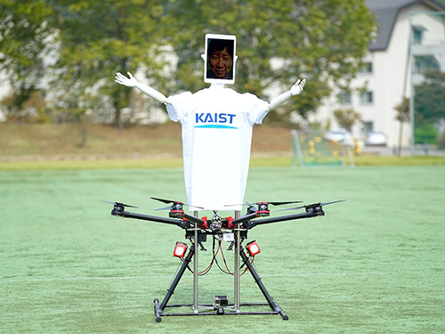 Robot Drone Man: A
Research Professor Ilhan Bae of the Moon Soul Graduate School of Future Strategy at KAIST created a life-size humanoid robot on a drone platform, which gives users the experience of virtual flight and an opportunity to interact with people at remote locations. Professor Bae calls his new creation a "telepresence robot."
This avatar drone is a new application of drone and robotics technology, which extends the reach of human presence and mobility, Professor Bae explained his research.
“As a futurist, I forecast that drone technology will soon evolve to become another body for humans, and I wanted to demonstrate this potential application of drones. Avatar drones are especially useful for people who need to meet or manage other people face to face in remote locations,” he said.
For example, if elderly people with physical disabilities want to engage in social gatherings, this avatar drone is designed to help them do just that.
For more details, please see the link below:
Behind the Music: How Robot Drone Man Built His Flying Avatar
IEEE Spectrum, November 7, 2016
2016.11.08 View 6769
Robot Drone Man: A
Research Professor Ilhan Bae of the Moon Soul Graduate School of Future Strategy at KAIST created a life-size humanoid robot on a drone platform, which gives users the experience of virtual flight and an opportunity to interact with people at remote locations. Professor Bae calls his new creation a "telepresence robot."
This avatar drone is a new application of drone and robotics technology, which extends the reach of human presence and mobility, Professor Bae explained his research.
“As a futurist, I forecast that drone technology will soon evolve to become another body for humans, and I wanted to demonstrate this potential application of drones. Avatar drones are especially useful for people who need to meet or manage other people face to face in remote locations,” he said.
For example, if elderly people with physical disabilities want to engage in social gatherings, this avatar drone is designed to help them do just that.
For more details, please see the link below:
Behind the Music: How Robot Drone Man Built His Flying Avatar
IEEE Spectrum, November 7, 2016
2016.11.08 View 6769 -
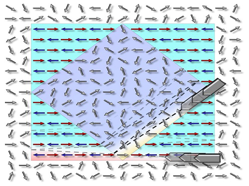 Technology to Allow Non-Magnetic Materials to Have Magnetic Properties by Professor Chan-Ho Yang
Professor Chan-Ho Yang and his research team from the Department of Physics at KAIST have developed a technology that allows non-magnetic materials to have magnetic properties or, in reverse, to remove magnetic properties from a magnet using an electric field.
Based on this research, it is expected that if magnetic-material-based data storage is developed, applications for high-speed massive data transfer will be possible.
The results of this research, with Ph.D. candidate Byung-Kwon Jang as the first author, were published online in Nature Physics on October 3.
Very small magnets exist inside of any materials. If the direction of the minuscule magnets is dis-aligned, pointing multiple directions, it is non-magnetic. If the direction is aligned in a certain direction, the material holds magnetic property just like any magnet we normally see.
Data storage capacity technology has rapidly advanced to the point where we can easily get a portable hard disk drive (HDD) with terabyte-level storage; however, the increase in storage is inevitably followed by slower data access speed for a storage device. Although HDDs are currently the most widely used data storage devices, their technical applications are limited due to their slow data access speed.
Other methods such as solid-state drives (SSDs), floating gates, and resistive switching have been developed as alternatives. Yet, they leave tracks every time data is written, and this can cause fatigue cumulative damage.
There have been many attempts to compose cells—the smallest data storage space on a storage device—with magnetic materials as that would enable faster data access speeds and remove fatigue cumulative damage. Generally, the techniques tried by researchers were to use induced magnetic fields through current flow. However, magnetic fields are very difficult to shield and can affect a large area. As a result, they alternate the magnetic property of adjacent cells. Because each cell cannot be adjusted one by one, it cannot also be arranged in a certain direction, and therefore, it is hard to change the magnetic state.
Professor Yang and his team adjusted the magnetic state by using magnetoelectric interaction to deal with this issue. Instead of using magnetic fields, magnetoelectric interaction is a method that uses an electric field to adjust the magnetic state. It has the advantage of smaller energy consumption as well.
Professor Yang's team demonstrated that cells facing random directions can be arranged in a certain direction by only inducing an electric field. In addition, the reverse was also proved to be feasible.
Until this research, most cases of previous findings were only feasible at extremely low temperatures or high temperatures, but the technology developed by the research team is practicable at room temperature by manipulating chemical pressure. It allows for a reversible magnetic state, and moreover, is non-volatile. Therefore, the results of this research are expected to provide the basis for developing next-generation information storage device.
Professor Yang said, “The changes in the electric magnetic state will be accompanied by entropy changes” and added, “Our research is expected to open new potential for future applications not only for magnetoelectric devices, but also for thermoelectric effect.”
This research has been worked on jointly with Dr. Si-Yong Choi from the Korea Institute of Materials Science, Prof. Yoon-Hee Jeong from the Pohang University of Science and Technology, Dr. Tae-Yeong Koo from the Pohang Accelerator Laboratory, Dr. Kyung-Tae Ko from the Max Planck Institute for Chemical Physics of Solids, Dr. Jun-Sik Lee and Dr. Hendrik Ohldag from the SLAC National Accelerator Laboratory of the United States, and Prof. Jan Seidel from the University of New South Wales of Australia.
The research was supported by the Mid-Career Researcher Program of the National Research Foundation of Korea, Global Research Network Support Project, Leading Research Center Support Project (Condensed Quantum Coherence Research Center), Global Frontier Project (Hybrid Interface Materials Research Group), and others.
Picture: The concept graphic for the electric-field-induced magnetic phase switching the magnetic direction
2016.11.04 View 8837
Technology to Allow Non-Magnetic Materials to Have Magnetic Properties by Professor Chan-Ho Yang
Professor Chan-Ho Yang and his research team from the Department of Physics at KAIST have developed a technology that allows non-magnetic materials to have magnetic properties or, in reverse, to remove magnetic properties from a magnet using an electric field.
Based on this research, it is expected that if magnetic-material-based data storage is developed, applications for high-speed massive data transfer will be possible.
The results of this research, with Ph.D. candidate Byung-Kwon Jang as the first author, were published online in Nature Physics on October 3.
Very small magnets exist inside of any materials. If the direction of the minuscule magnets is dis-aligned, pointing multiple directions, it is non-magnetic. If the direction is aligned in a certain direction, the material holds magnetic property just like any magnet we normally see.
Data storage capacity technology has rapidly advanced to the point where we can easily get a portable hard disk drive (HDD) with terabyte-level storage; however, the increase in storage is inevitably followed by slower data access speed for a storage device. Although HDDs are currently the most widely used data storage devices, their technical applications are limited due to their slow data access speed.
Other methods such as solid-state drives (SSDs), floating gates, and resistive switching have been developed as alternatives. Yet, they leave tracks every time data is written, and this can cause fatigue cumulative damage.
There have been many attempts to compose cells—the smallest data storage space on a storage device—with magnetic materials as that would enable faster data access speeds and remove fatigue cumulative damage. Generally, the techniques tried by researchers were to use induced magnetic fields through current flow. However, magnetic fields are very difficult to shield and can affect a large area. As a result, they alternate the magnetic property of adjacent cells. Because each cell cannot be adjusted one by one, it cannot also be arranged in a certain direction, and therefore, it is hard to change the magnetic state.
Professor Yang and his team adjusted the magnetic state by using magnetoelectric interaction to deal with this issue. Instead of using magnetic fields, magnetoelectric interaction is a method that uses an electric field to adjust the magnetic state. It has the advantage of smaller energy consumption as well.
Professor Yang's team demonstrated that cells facing random directions can be arranged in a certain direction by only inducing an electric field. In addition, the reverse was also proved to be feasible.
Until this research, most cases of previous findings were only feasible at extremely low temperatures or high temperatures, but the technology developed by the research team is practicable at room temperature by manipulating chemical pressure. It allows for a reversible magnetic state, and moreover, is non-volatile. Therefore, the results of this research are expected to provide the basis for developing next-generation information storage device.
Professor Yang said, “The changes in the electric magnetic state will be accompanied by entropy changes” and added, “Our research is expected to open new potential for future applications not only for magnetoelectric devices, but also for thermoelectric effect.”
This research has been worked on jointly with Dr. Si-Yong Choi from the Korea Institute of Materials Science, Prof. Yoon-Hee Jeong from the Pohang University of Science and Technology, Dr. Tae-Yeong Koo from the Pohang Accelerator Laboratory, Dr. Kyung-Tae Ko from the Max Planck Institute for Chemical Physics of Solids, Dr. Jun-Sik Lee and Dr. Hendrik Ohldag from the SLAC National Accelerator Laboratory of the United States, and Prof. Jan Seidel from the University of New South Wales of Australia.
The research was supported by the Mid-Career Researcher Program of the National Research Foundation of Korea, Global Research Network Support Project, Leading Research Center Support Project (Condensed Quantum Coherence Research Center), Global Frontier Project (Hybrid Interface Materials Research Group), and others.
Picture: The concept graphic for the electric-field-induced magnetic phase switching the magnetic direction
2016.11.04 View 8837 -
 2016 KAIST EEWS Workshop
The Energy, Environment, Water and Sustainability (EEWS) Graduate School of KAIST hosted a workshop entitled “Progress and Perspectives of Energy Science and Technology” on October 20, 2016. The workshop took place at the Fusion Hall of the KAIST Institute on campus.
About 400 experts in energy science and engineering participated in the event. Eight globally recognized scientists introduced the latest research trends in nanomaterials, energy theory, catalysts, and photocatalysts and led discussions on the current status and prospects of EEWS.
Professors Yi Cui of Stanford University, an expert in nanomaterials, and William A. Goddard of California Institute of Technology presented their research experiments on materials design and recent results on the direction of theory under the topics of energy and environment.
Dr. Miquel Salmeron, a former head of the Material Science Division of Lawrence Berkeley National Laboratory, and Professor Yuichi Ikuhara of Tokyo University introduced their analysis of catalysts and energy matters at an atomic scale.
Professor Sukbok Chang of the Chemistry Department at KAIST, a deputy editor of ACS Catalysis and the head of the Center for Catalytic Hydrocarbon Functionalizations at the Institute of Basic Science, and Professor Yang-Kook Sun of Energy Engineering at Hanyang University, who is also a deputy editor of ACS Energy Letters, presented their latest research results on new catalytic reaction development and energy storage.
The workshop consisted of three sections which addressed the design of energy and environment materials; analysis of energy and catalytic materials; and energy conversion and catalysts.
The EEWS Graduate School was established in 2008 with the sponsorship of the Korean government’s World Class University (WCU) project to support science education in Korea. Professor J. Fraser Stoddart, the winner of the 2016 Nobel Prize in Chemistry, was previously worked at the KAIST EEWS Graduate School as a WCU visiting professor for two years, from 2011 to 2013. Professor Ali Coskun, who was a postdoctoral researcher in the laboratory of Professor Stoddart, now teaches and conducts research as a full-time professor at the graduate school.
Dean Yousung Jung of the EEWS Graduate School said:
“This workshop has provided us with a meaningful opportunity to engage in discussions on energy science and technology with world-class scholars from all around the world. It is also a good venue for our graduate school to share with them what we have been doing in research and education.”
2016.10.20 View 15180
2016 KAIST EEWS Workshop
The Energy, Environment, Water and Sustainability (EEWS) Graduate School of KAIST hosted a workshop entitled “Progress and Perspectives of Energy Science and Technology” on October 20, 2016. The workshop took place at the Fusion Hall of the KAIST Institute on campus.
About 400 experts in energy science and engineering participated in the event. Eight globally recognized scientists introduced the latest research trends in nanomaterials, energy theory, catalysts, and photocatalysts and led discussions on the current status and prospects of EEWS.
Professors Yi Cui of Stanford University, an expert in nanomaterials, and William A. Goddard of California Institute of Technology presented their research experiments on materials design and recent results on the direction of theory under the topics of energy and environment.
Dr. Miquel Salmeron, a former head of the Material Science Division of Lawrence Berkeley National Laboratory, and Professor Yuichi Ikuhara of Tokyo University introduced their analysis of catalysts and energy matters at an atomic scale.
Professor Sukbok Chang of the Chemistry Department at KAIST, a deputy editor of ACS Catalysis and the head of the Center for Catalytic Hydrocarbon Functionalizations at the Institute of Basic Science, and Professor Yang-Kook Sun of Energy Engineering at Hanyang University, who is also a deputy editor of ACS Energy Letters, presented their latest research results on new catalytic reaction development and energy storage.
The workshop consisted of three sections which addressed the design of energy and environment materials; analysis of energy and catalytic materials; and energy conversion and catalysts.
The EEWS Graduate School was established in 2008 with the sponsorship of the Korean government’s World Class University (WCU) project to support science education in Korea. Professor J. Fraser Stoddart, the winner of the 2016 Nobel Prize in Chemistry, was previously worked at the KAIST EEWS Graduate School as a WCU visiting professor for two years, from 2011 to 2013. Professor Ali Coskun, who was a postdoctoral researcher in the laboratory of Professor Stoddart, now teaches and conducts research as a full-time professor at the graduate school.
Dean Yousung Jung of the EEWS Graduate School said:
“This workshop has provided us with a meaningful opportunity to engage in discussions on energy science and technology with world-class scholars from all around the world. It is also a good venue for our graduate school to share with them what we have been doing in research and education.”
2016.10.20 View 15180