Ro
-
 Highly Scalable Process to Obtain Stable 2D Nanosheet Dispersion
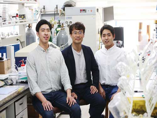
(Professor Do Hyun Kim and his team)
A KAIST team developed technology that allows the mass production of two-dimensional (2D) nanomaterial dispersion by utilizing the characteristic shearing force of hydraulic power.
The 2D nanosheet dispersion can be directly applied to solution-based processes to manufacture devices for electronics as well as energy storage and conversion. It is expected to be used in these devices with improved performance.
There have been numerous researches on the mass production of various 2D nanomaterial because they show outstanding physical and chemical characteristics when they are truly 2D.
With strong mechanical force or chemical reaction only, each existing exfoliation method has its limitation to make 2D material when the scale of manufacturing increases. They also face the issues of high cost and long process time.
Moreover, 2D nanosheets by the exfoliation have the tendency of agglomeration due to the surface energy. Usually, organic solvent or surfactant is required to obtain high yield and concentration of 2D material by minimizing agglomeration.
After several years of research, Professor Do Hyun Kim in the Department of Chemical and Biomolecular Engineering and his team verified that optimized shearing in their reactor provided the highest efficiency for the exfoliation of nanomaterial. For the increased reactor capacity, they selected a flow and a dispersive agent to develop a high-speed, mass-production process to get 2D nanosheets by physical exfoliation with an aqueous solution.
The team proposed a flow reactor based on Taylor-Couette flow, which has the advantage of high shear rate and mixing efficiency even under large reactor capacity.
In this research, Professor Young-Kyu Han at Dongguk University-Seoul carried out the Ab initio calculation to select the dispersive agent. According to his calculation, an ionic liquid can stabilize and disperse 2D nanomaterial even in a small concentration. This calculation could maximize the exfoliating efficiency.
Professor Bong Gill Choi at Kangwon National University carried out the evaluation of device made of resulting dispersion. The team used a membrane filtration process to make a flexible and highly conductive film of 2D material. The film was then applied to produce an electrode for the supercapacitor device with very high capacity per volume. They also confirmed its stability in their supercapacitor device.
Additionally, they applied dispersive nanomaterials including graphene, molybdenum disulfide (MoS₂), and boron nitride (BN) to inkjet printer ink and realized micrometer-thick nanomaterial patterns on A4 paper. The graphene ink showed no loss of electrical property after printing without additional heat treatment.
Professor Kim said, “This new technology for the high-speed mass production of nanomaterials can easily be applied to various 2D nanomaterials. It will accelerate the production of highly efficient devices for optoelectronics, biosensors, and energy storage/conversion units with low cost.”
This research, led by Dr. Jae-Min Jeong, was published in Advanced Functional Materials on August 12.
Figure 1. The cover page of Advanced Functional Materials
2018.12.19 View 6537
Highly Scalable Process to Obtain Stable 2D Nanosheet Dispersion
(Professor Do Hyun Kim and his team)
A KAIST team developed technology that allows the mass production of two-dimensional (2D) nanomaterial dispersion by utilizing the characteristic shearing force of hydraulic power.
The 2D nanosheet dispersion can be directly applied to solution-based processes to manufacture devices for electronics as well as energy storage and conversion. It is expected to be used in these devices with improved performance.
There have been numerous researches on the mass production of various 2D nanomaterial because they show outstanding physical and chemical characteristics when they are truly 2D.
With strong mechanical force or chemical reaction only, each existing exfoliation method has its limitation to make 2D material when the scale of manufacturing increases. They also face the issues of high cost and long process time.
Moreover, 2D nanosheets by the exfoliation have the tendency of agglomeration due to the surface energy. Usually, organic solvent or surfactant is required to obtain high yield and concentration of 2D material by minimizing agglomeration.
After several years of research, Professor Do Hyun Kim in the Department of Chemical and Biomolecular Engineering and his team verified that optimized shearing in their reactor provided the highest efficiency for the exfoliation of nanomaterial. For the increased reactor capacity, they selected a flow and a dispersive agent to develop a high-speed, mass-production process to get 2D nanosheets by physical exfoliation with an aqueous solution.
The team proposed a flow reactor based on Taylor-Couette flow, which has the advantage of high shear rate and mixing efficiency even under large reactor capacity.
In this research, Professor Young-Kyu Han at Dongguk University-Seoul carried out the Ab initio calculation to select the dispersive agent. According to his calculation, an ionic liquid can stabilize and disperse 2D nanomaterial even in a small concentration. This calculation could maximize the exfoliating efficiency.
Professor Bong Gill Choi at Kangwon National University carried out the evaluation of device made of resulting dispersion. The team used a membrane filtration process to make a flexible and highly conductive film of 2D material. The film was then applied to produce an electrode for the supercapacitor device with very high capacity per volume. They also confirmed its stability in their supercapacitor device.
Additionally, they applied dispersive nanomaterials including graphene, molybdenum disulfide (MoS₂), and boron nitride (BN) to inkjet printer ink and realized micrometer-thick nanomaterial patterns on A4 paper. The graphene ink showed no loss of electrical property after printing without additional heat treatment.
Professor Kim said, “This new technology for the high-speed mass production of nanomaterials can easily be applied to various 2D nanomaterials. It will accelerate the production of highly efficient devices for optoelectronics, biosensors, and energy storage/conversion units with low cost.”
This research, led by Dr. Jae-Min Jeong, was published in Advanced Functional Materials on August 12.
Figure 1. The cover page of Advanced Functional Materials
2018.12.19 View 6537 -
 Characteristics of Submesoscale Geophysical Turbulence Reported
A KAIST research team has reported some of unique characteristics and driving forces behind submesoscale geophysical turbulence. Using big data analysis on ocean surface currents and chlorophyll concentrations observed using coastal radars and satellites has brought better understanding of oceanic processes in space and time scales of O(1) kilometer and O(1) hour. The outcomes of this work will lead to improved tracking of water-borne materials and performance in global and regional climate prediction models.
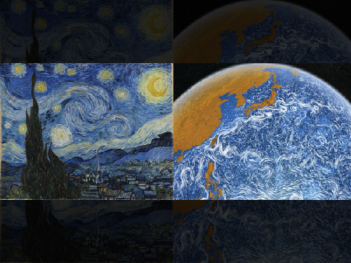
In 2012, United States National Aeronautics and Space Administration (NASA) released a movie clip called “Perpetual Oceans”, which visualized ocean circulation obtained from satellite altimeter-derived sea surface height observations over two and a half years. When the movie was released to the public, it received a great deal of attention because the circulation patterns were strikingly similar to “The Starry Night” by Vincent van Gogh.
“Perpetual Oceans” is full of vortical flow patterns describing the oceanic turbulent motions at mesoscale (a scale of 100 km or larger). Meanwhile, Professor Sung Yong Kim from the Department of Mechanical Engineering and his team focused on the study of the oceanic turbulence at sub-mesoscale (space and time scales of 1 to 100 km and hours).
Sub-mesoscale processes are important because they contribute to the vertical transport of oceanic tracers, mass, buoyancy, and nutrients and rectify both the mixed layer structure and upper ocean stratification. These process studies have been primarily based on numerical simulations because traditional in situ ocean measurements can be limited in their capability to resolve the detailed horizontal and vertical structures of these processes.
The team conducted big data analysis on hourly observations of one-year ocean surface current maps and five-year chlorophyll concentration maps, obtained from remote sensing instruments such as coastal high-frequency radars (HFRs) and geostationary ocean color imagery (GOCI) to examine the unique characteristics of oceanic submesoscale processes.
The team analyzed the slope change of the wavenumber energy spectra of the observations in terms of season and sampling directions. Through the analysis, the team proved that energy cascade (a phenomenon in which large-scale energy transfers to small-scale energy or vice-versa during the turbulent energy transit) occurs in the spatial scale of 10 km in the forward and inverse directions. This is driven by baroclinic instability as opposed to the mesoscale eddy-driven frontogenesis at the O(100) km scale based on the observed regional submesoscale circulations.
This work will contribute to the parameterization of physical phenomenon of sub-mesoscale in the field of global high-resolution modeling within ocean physics and atmospheric as well as climate change. Based on the understanding of the principle of sub-mesoscale surface circulation, practical applications can be further derived for radioactivity, oil spill recovery, and marine pollutant tracking.
Moreover, the data used in this research was based on long-term observations on sub-mesoscale surface currents and concentrations of chlorophyll, which may reflect the submesoscale processes actively generated in the subpolar front off the east coast of Korea. Hence, this study can potentially be beneficial for integrated big data analyses using high-resolution coastal radar-derived surface currents and satellite-derived products and motivate interdisciplinary research between ocean physics and biology.
This research was published as two companion papers in the Journal of Geophysical Research: Oceans on August 6, 2018. (doi:10.1002/2016JC012517; doi:10.1002/2017JC013732)
Figure 1.'The Starry Night' of Van Gogh and the 'Perpetual Ocean' created by NASA's Goddard Space Flight Center.
Figure 2. A schematic diagram of the energy cascades in forward and backward directions and the spatial scale where the energy is injected.
Figure 3. A snapshot of the chlorophyll concentration map derived from geostationary ocean color imagery (GOCI) off the east coast of Korea presenting several examples of sub-mesoscale turbulent flows.
Figure 4. Energy spectra of the HFR-derived surface currents and GOCI-derived chlorophyll concentrations and the temporal variability of spectral decay slopes in the cross-shore and along-shore directions.
2018.12.13 View 6189
Characteristics of Submesoscale Geophysical Turbulence Reported
A KAIST research team has reported some of unique characteristics and driving forces behind submesoscale geophysical turbulence. Using big data analysis on ocean surface currents and chlorophyll concentrations observed using coastal radars and satellites has brought better understanding of oceanic processes in space and time scales of O(1) kilometer and O(1) hour. The outcomes of this work will lead to improved tracking of water-borne materials and performance in global and regional climate prediction models.
In 2012, United States National Aeronautics and Space Administration (NASA) released a movie clip called “Perpetual Oceans”, which visualized ocean circulation obtained from satellite altimeter-derived sea surface height observations over two and a half years. When the movie was released to the public, it received a great deal of attention because the circulation patterns were strikingly similar to “The Starry Night” by Vincent van Gogh.
“Perpetual Oceans” is full of vortical flow patterns describing the oceanic turbulent motions at mesoscale (a scale of 100 km or larger). Meanwhile, Professor Sung Yong Kim from the Department of Mechanical Engineering and his team focused on the study of the oceanic turbulence at sub-mesoscale (space and time scales of 1 to 100 km and hours).
Sub-mesoscale processes are important because they contribute to the vertical transport of oceanic tracers, mass, buoyancy, and nutrients and rectify both the mixed layer structure and upper ocean stratification. These process studies have been primarily based on numerical simulations because traditional in situ ocean measurements can be limited in their capability to resolve the detailed horizontal and vertical structures of these processes.
The team conducted big data analysis on hourly observations of one-year ocean surface current maps and five-year chlorophyll concentration maps, obtained from remote sensing instruments such as coastal high-frequency radars (HFRs) and geostationary ocean color imagery (GOCI) to examine the unique characteristics of oceanic submesoscale processes.
The team analyzed the slope change of the wavenumber energy spectra of the observations in terms of season and sampling directions. Through the analysis, the team proved that energy cascade (a phenomenon in which large-scale energy transfers to small-scale energy or vice-versa during the turbulent energy transit) occurs in the spatial scale of 10 km in the forward and inverse directions. This is driven by baroclinic instability as opposed to the mesoscale eddy-driven frontogenesis at the O(100) km scale based on the observed regional submesoscale circulations.
This work will contribute to the parameterization of physical phenomenon of sub-mesoscale in the field of global high-resolution modeling within ocean physics and atmospheric as well as climate change. Based on the understanding of the principle of sub-mesoscale surface circulation, practical applications can be further derived for radioactivity, oil spill recovery, and marine pollutant tracking.
Moreover, the data used in this research was based on long-term observations on sub-mesoscale surface currents and concentrations of chlorophyll, which may reflect the submesoscale processes actively generated in the subpolar front off the east coast of Korea. Hence, this study can potentially be beneficial for integrated big data analyses using high-resolution coastal radar-derived surface currents and satellite-derived products and motivate interdisciplinary research between ocean physics and biology.
This research was published as two companion papers in the Journal of Geophysical Research: Oceans on August 6, 2018. (doi:10.1002/2016JC012517; doi:10.1002/2017JC013732)
Figure 1.'The Starry Night' of Van Gogh and the 'Perpetual Ocean' created by NASA's Goddard Space Flight Center.
Figure 2. A schematic diagram of the energy cascades in forward and backward directions and the spatial scale where the energy is injected.
Figure 3. A snapshot of the chlorophyll concentration map derived from geostationary ocean color imagery (GOCI) off the east coast of Korea presenting several examples of sub-mesoscale turbulent flows.
Figure 4. Energy spectra of the HFR-derived surface currents and GOCI-derived chlorophyll concentrations and the temporal variability of spectral decay slopes in the cross-shore and along-shore directions.
2018.12.13 View 6189 -
 From Concept to Reality: Changing Color of Light Using a Spatiotemporal Boundary
(from left: Professor Bumki Min, PhD candidate Jaehyeon Son and PhD Kanghee Lee)
A KAIST team developed an optical technique to change the color (frequency) of light using a spatiotemporal boundary. The research focuses on realizing a spatiotemporal boundary with a much higher degree of freedom than the results of previous studies by fabricating a thin metal structure on a semiconductor surface. Such a spatiotemporal boundary is expected to be applicable to an ultra-thin film type optical device capable of changing the color of light.
The optical frequency conversion device plays a key role in precision measurement and communication technology, and the device has been developed mainly based on optical nonlinearity.
If the intensity of light is very strong, the optical medium responds nonlinearly so the nonlinear optical phenomena, such as frequency doubling or frequency mixing, can be observed. Such optical nonlinear phenomena are realized usually by the interaction between a high-intensity laser and a nonlinear medium.
As an alternative method frequency conversion is observed by temporally modifying the optical properties of the medium through which light travels using an external stimulus. Since frequency conversion in this way can be observed even in weak light, such a technique could be particularly useful in communication technology.
However, rapid optical property modification of the medium by an external stimulus and subsequent light frequency conversion techniques have been researched only in the pertubative regime, and it has been difficult to realize these theoretical results in practical applications.
To realize such a conceptual idea, Professor Bumki Min from the Department of Mechanical Engineering and his team collaborated with Professor Wonju Jeon from the Department of Mechanical Engineering and Professor Fabian Rotermund from the Department of Physics. They developed an artificial optical material (metamaterial) by arranging a metal microstructure that mimics an atomic structure and succeeded in creating a spatiotemporal boundary by changing the optical property of the artificial material abruptly.
While previous studies only slightly modified the refractive index of the medium, this study provided a spatiotemporal boundary as a platform for freely designing and changing the spectral properties of the medium. Using this, the research team developed a device that can control the frequency of light to a large degree.
The research team said a spatiotemporal boundary, which was only conceptually considered in previous research and realized in the pertubative regime, was developed as a step that can be realized and applied.
Professor Min said, “The frequency conversion of light becomes designable and predictable, so our research could be applied in many optical applications. This research will present a new direction for time-variant media research projects in the field of optics.”
This research, led by PhD Kanghee Lee and PhD candidate Jaehyeon Son, was published online in Nature Photonics on October 8, 2018.
This work was supported by the National Research Foundation of Korea (NRF) through the government of Korea. The work was also supported by the Center for Advanced Meta-Materials (CAMM) funded by the Korea Government (MSIP) as the Global Frontier Project (NRF-2014M3A6B3063709).
Figure 1. The frequency conversion process of light using a spatiotemporal boundary.
Figure 2. The complex amplitude of light at the converted frequency with the variation of a spatiotemporal boundary.
2018.11.29 View 9248
From Concept to Reality: Changing Color of Light Using a Spatiotemporal Boundary
(from left: Professor Bumki Min, PhD candidate Jaehyeon Son and PhD Kanghee Lee)
A KAIST team developed an optical technique to change the color (frequency) of light using a spatiotemporal boundary. The research focuses on realizing a spatiotemporal boundary with a much higher degree of freedom than the results of previous studies by fabricating a thin metal structure on a semiconductor surface. Such a spatiotemporal boundary is expected to be applicable to an ultra-thin film type optical device capable of changing the color of light.
The optical frequency conversion device plays a key role in precision measurement and communication technology, and the device has been developed mainly based on optical nonlinearity.
If the intensity of light is very strong, the optical medium responds nonlinearly so the nonlinear optical phenomena, such as frequency doubling or frequency mixing, can be observed. Such optical nonlinear phenomena are realized usually by the interaction between a high-intensity laser and a nonlinear medium.
As an alternative method frequency conversion is observed by temporally modifying the optical properties of the medium through which light travels using an external stimulus. Since frequency conversion in this way can be observed even in weak light, such a technique could be particularly useful in communication technology.
However, rapid optical property modification of the medium by an external stimulus and subsequent light frequency conversion techniques have been researched only in the pertubative regime, and it has been difficult to realize these theoretical results in practical applications.
To realize such a conceptual idea, Professor Bumki Min from the Department of Mechanical Engineering and his team collaborated with Professor Wonju Jeon from the Department of Mechanical Engineering and Professor Fabian Rotermund from the Department of Physics. They developed an artificial optical material (metamaterial) by arranging a metal microstructure that mimics an atomic structure and succeeded in creating a spatiotemporal boundary by changing the optical property of the artificial material abruptly.
While previous studies only slightly modified the refractive index of the medium, this study provided a spatiotemporal boundary as a platform for freely designing and changing the spectral properties of the medium. Using this, the research team developed a device that can control the frequency of light to a large degree.
The research team said a spatiotemporal boundary, which was only conceptually considered in previous research and realized in the pertubative regime, was developed as a step that can be realized and applied.
Professor Min said, “The frequency conversion of light becomes designable and predictable, so our research could be applied in many optical applications. This research will present a new direction for time-variant media research projects in the field of optics.”
This research, led by PhD Kanghee Lee and PhD candidate Jaehyeon Son, was published online in Nature Photonics on October 8, 2018.
This work was supported by the National Research Foundation of Korea (NRF) through the government of Korea. The work was also supported by the Center for Advanced Meta-Materials (CAMM) funded by the Korea Government (MSIP) as the Global Frontier Project (NRF-2014M3A6B3063709).
Figure 1. The frequency conversion process of light using a spatiotemporal boundary.
Figure 2. The complex amplitude of light at the converted frequency with the variation of a spatiotemporal boundary.
2018.11.29 View 9248 -
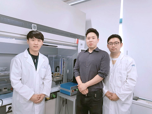
 Silk Adhesive Paves the Way for Epidermal Electronics
(from left: Dr. Ji-Won Seo, Professor Hyunjoo Jenny Lee and PhD candidate, Hyojung Kim)
Producing effective epidermal electronics requires a strong, biocompatible interface between a biological surface and a sensor. Here, a KAIST team employed a calcium-modified silk fibroin as a biocompatible and strong adhesive. This technology led to the development of epidermal electronics with strong adhesion for patients who need drug injections and physiological monitoring over a long time.
Recently, biocompatible silk fibroins has been increasingly used for flexible substrates and water-soluble sacrificial layers because they allow structural modifications and are biodegradable. From previous studies, the team discovered the adhesive properties of silk fibroin via metal chelate bonding and the water-capturing of Ca ions.
Professor Hyunjoo Jenny Lee from the School of Electrical Engineering and her team explored ways to develop reusable, water-degradable, biocompatible and conductive epidermal electronics that can be attached to the human skin for long-term use. To overcome the limitations of conventional silk fibroin, the team introduced Ca ions to modify silk fibroin into a strong and biocompatible adhesive.
Calcium ions adopted in silk fibroins serve to capture water and enhance the cohesion force through metal chelation. Therefore, this endows viscoelasticity to previously a firm silk fibroin. This modified silk fibroin exhibits strong viscoelasticity and strong adhesiveness when physically attached to the human skin and various polymer substrates. Their developed silk adhesive is reusable, water-degradable, biocompatible, and conductive.
To test the effectiveness, the team employed the silk adhesive to fabricate an epidermal capacitive touch sensor that can be attached to the human skin. They verified the reusability of the sensor by performing attachment and detachment tests. They also confirmed that the physical adhesion of the Ca-modified silk facilitates its reusability and possesses high peel strength.
Furthermore, they tested the stretchability of the silk adhesive on bladder tissue. Although it is not an epidermal skin, bladder tissue is highly stretchable. Hence, it is a perfect target to measure the resistance-strain characteristic of the silk adhesive. When the bladder tissue was stretched, the resistive strain epidermal sensor corresponded to the tensile strain.
Showing high biocompatibility, the silk adhesive is suitable for interfacing with the human skin for a long period of time. Therefore, it can also be applied to a drug delivery epidermal system as well as an electrocardiogram (ECG) epidermal sensor.
Professor Lee said, “We are opening up a novel use for silk by developing reusable and biodegradable silk adhesive using biocompatible silk fibroin. This technology will contribute to the development of next-generation epidermal electronics as well as drug delivery systems.
This research, led by Dr. Ji-Won Seo and a PhD candidate, Hyojung Kim, was published in Advanced Functional Materials on September 5, 2018.
Figure 1. Schematic and photograph of a hydrogel patch adhered on the human skin through the silk adhesive
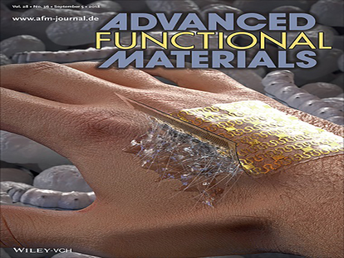
Figure 2. Cover page of Advanced Functional Materials
2018.11.21 View 7258
Silk Adhesive Paves the Way for Epidermal Electronics
(from left: Dr. Ji-Won Seo, Professor Hyunjoo Jenny Lee and PhD candidate, Hyojung Kim)
Producing effective epidermal electronics requires a strong, biocompatible interface between a biological surface and a sensor. Here, a KAIST team employed a calcium-modified silk fibroin as a biocompatible and strong adhesive. This technology led to the development of epidermal electronics with strong adhesion for patients who need drug injections and physiological monitoring over a long time.
Recently, biocompatible silk fibroins has been increasingly used for flexible substrates and water-soluble sacrificial layers because they allow structural modifications and are biodegradable. From previous studies, the team discovered the adhesive properties of silk fibroin via metal chelate bonding and the water-capturing of Ca ions.
Professor Hyunjoo Jenny Lee from the School of Electrical Engineering and her team explored ways to develop reusable, water-degradable, biocompatible and conductive epidermal electronics that can be attached to the human skin for long-term use. To overcome the limitations of conventional silk fibroin, the team introduced Ca ions to modify silk fibroin into a strong and biocompatible adhesive.
Calcium ions adopted in silk fibroins serve to capture water and enhance the cohesion force through metal chelation. Therefore, this endows viscoelasticity to previously a firm silk fibroin. This modified silk fibroin exhibits strong viscoelasticity and strong adhesiveness when physically attached to the human skin and various polymer substrates. Their developed silk adhesive is reusable, water-degradable, biocompatible, and conductive.
To test the effectiveness, the team employed the silk adhesive to fabricate an epidermal capacitive touch sensor that can be attached to the human skin. They verified the reusability of the sensor by performing attachment and detachment tests. They also confirmed that the physical adhesion of the Ca-modified silk facilitates its reusability and possesses high peel strength.
Furthermore, they tested the stretchability of the silk adhesive on bladder tissue. Although it is not an epidermal skin, bladder tissue is highly stretchable. Hence, it is a perfect target to measure the resistance-strain characteristic of the silk adhesive. When the bladder tissue was stretched, the resistive strain epidermal sensor corresponded to the tensile strain.
Showing high biocompatibility, the silk adhesive is suitable for interfacing with the human skin for a long period of time. Therefore, it can also be applied to a drug delivery epidermal system as well as an electrocardiogram (ECG) epidermal sensor.
Professor Lee said, “We are opening up a novel use for silk by developing reusable and biodegradable silk adhesive using biocompatible silk fibroin. This technology will contribute to the development of next-generation epidermal electronics as well as drug delivery systems.
This research, led by Dr. Ji-Won Seo and a PhD candidate, Hyojung Kim, was published in Advanced Functional Materials on September 5, 2018.
Figure 1. Schematic and photograph of a hydrogel patch adhered on the human skin through the silk adhesive
Figure 2. Cover page of Advanced Functional Materials
2018.11.21 View 7258 -
 Controlling Crystal Size of Organic Semiconductors
A KAIST research team led by Professor Steve Park from the Department of Materials Science and Engineering
Recently, solution-processable organic semiconductors are being highlighted for their potential application in printed electronics, becoming a feasible technique to fabricate large-area flexible thin film at a low cost. The field-effect mobility of small-molecule organic semiconductors is dependent on the crystallinity, crystal orientation, and crystal size. A variety of solution-based coating techniques, such as ink-jet printing, dip-coating, and solution shearing have been developed to control the crystallinity and crystal orientation, but a method for developing techniques to increase the crystal size of organic semiconductors is still needed.
To overcome this issue, the research team developed an inorganic polymer micropillar-based solution shearing system to increase the crystal size of an organic semiconductor with pillar size. Using this technique, the crystallization process of organic semiconductors can be controlled precisely, and therefore large-area organic semiconductor thin film with controlled crystallinity can be fabricated.
A variety of solution-based coating techniques cannot control the fluid-flow of solutions appropriately, so the solvent evaporates randomly onto the substrate, which has difficulty in the fabrication of organic semiconductor thin film with a large crystal size.
The research team integrated inorganic polymer microstructures into the solution shearing blade to solve this issue. The inorganic polymer can easily be microstructured via conventional molding techniques, has high mechanical durability, and organic solvent resistance. Using the inorganic polymer-based microstructure blade, the research team controlled the size of small molecule organic semiconductors by tuning the shape and dimensions of the microstructure. The microstructures in the blade induce the sharp curvature regions in the meniscus line that formed between the shearing blade and the substrate, and therefore nucleation and crystal growth can be regulated. Hence, the research team fabricated organic semiconductor thin-film with large crystals, which increases the field-effect mobility.
The research team also demonstrated a solution shearing process on a curved surface by using a flexible inorganic polymer-based shearing blade, which expands the applicability of solution shearing.
Professor Park said, “Our new solution shearing system can control the crystallization process precisely during solvent evaporation.” He added, “This technique adds another key parameter that can be utilized to tune the property of thin films and opens up a wide variety of new applications.
The results of this work entitled “Inorganic Polymer Micropillar-Based Solution Shearing of Large-Area Organic Semiconductor Thin Films with Pillar-Size-Dependent Crystal Size” was published in the July 2018 issue of Advanced Materials as a cover article.
2018.10.30 View 6959
Controlling Crystal Size of Organic Semiconductors
A KAIST research team led by Professor Steve Park from the Department of Materials Science and Engineering
Recently, solution-processable organic semiconductors are being highlighted for their potential application in printed electronics, becoming a feasible technique to fabricate large-area flexible thin film at a low cost. The field-effect mobility of small-molecule organic semiconductors is dependent on the crystallinity, crystal orientation, and crystal size. A variety of solution-based coating techniques, such as ink-jet printing, dip-coating, and solution shearing have been developed to control the crystallinity and crystal orientation, but a method for developing techniques to increase the crystal size of organic semiconductors is still needed.
To overcome this issue, the research team developed an inorganic polymer micropillar-based solution shearing system to increase the crystal size of an organic semiconductor with pillar size. Using this technique, the crystallization process of organic semiconductors can be controlled precisely, and therefore large-area organic semiconductor thin film with controlled crystallinity can be fabricated.
A variety of solution-based coating techniques cannot control the fluid-flow of solutions appropriately, so the solvent evaporates randomly onto the substrate, which has difficulty in the fabrication of organic semiconductor thin film with a large crystal size.
The research team integrated inorganic polymer microstructures into the solution shearing blade to solve this issue. The inorganic polymer can easily be microstructured via conventional molding techniques, has high mechanical durability, and organic solvent resistance. Using the inorganic polymer-based microstructure blade, the research team controlled the size of small molecule organic semiconductors by tuning the shape and dimensions of the microstructure. The microstructures in the blade induce the sharp curvature regions in the meniscus line that formed between the shearing blade and the substrate, and therefore nucleation and crystal growth can be regulated. Hence, the research team fabricated organic semiconductor thin-film with large crystals, which increases the field-effect mobility.
The research team also demonstrated a solution shearing process on a curved surface by using a flexible inorganic polymer-based shearing blade, which expands the applicability of solution shearing.
Professor Park said, “Our new solution shearing system can control the crystallization process precisely during solvent evaporation.” He added, “This technique adds another key parameter that can be utilized to tune the property of thin films and opens up a wide variety of new applications.
The results of this work entitled “Inorganic Polymer Micropillar-Based Solution Shearing of Large-Area Organic Semiconductor Thin Films with Pillar-Size-Dependent Crystal Size” was published in the July 2018 issue of Advanced Materials as a cover article.
2018.10.30 View 6959 -
 Lens-free OLEDs with Efficiency comparable to that of Inorganic LEDs
(from left: Professor Seunghyup Yoo and PhD candidate Jinouk Song)
The use of organic light-emitting diodes (OLEDs) has extended to various applications, but their efficiency is still lagging behind inorganic light-emitting diodes. In this research, a KAIST team provided a systematic way to yield OLEDs with an external quantum efficiency (EQE) greater than 50% with an external scattering medium.
Having properties suitable for thin and flexible devices, OLEDs are popular light sources for displays, such as mobile devices and high quality TVs. In recent years, numerous efforts have been made to apply OLEDs in lighting as well as light sources for vehicles.
For such applications, high efficiency is of the upmost importance for the successful deployment of light sources. Thanks to continuous research and the development of OLEDs, their efficiency is steadily on the rise, and a level equivalent to inorganic LEDs has been demonstrated in some reports.
However, these highly efficient OLEDs were often achieved with a macroscopic lens or complex internal nanostructures, which undermines the key advantages of OLEDs as an affordable planar light sources and tends to hinder their stable operation, thus putting a limitation to their commercialization.
Among various methods proven effective for OLED light extraction, a team led by Professor Seunghyup Yoo at the School of Electrical Engineering focused on the external scattering-based approach, as it can maintain planar geometry and compatibility with flexibility. It is also able to be fabricated on a large scale at a low cost and causes no interference with electrical properties of OLEDs.
Conventionally, research on enhancing OLED light extraction using light scattering has been conducted empirically in many cases. This time, the team developed comprehensive and analytical methodology to theoretically predict structures that maximize efficiency.
Considering OLEDs with the external scattering layers as a whole rather than two separate entities, the researchers combined the mathematical description of the scattering phenomena with the optical model for light emission within an OLED to rapidly predict the characteristics of many devices with various structures. Based on this approach, the team theoretically predicted the optimal combination of scattering layers and OLED architectures that can lead to the maximum efficiency.
Following this theoretical prediction, the team experimentally produced the optimal light scattering film and incorporated it to OLEDs with orange emitters having a high degree of horizontal dipole orientation. As a result, the team successfully realized OLEDs exhibiting EQE of 56% and power efficiency of 221 lm/W. This is one of the highest efficiencies ever realized for an OLED unit device without the help of a macroscopic lens or internal light extraction structures.
Professor Yoo said, “There are various technologies developed for improving OLED light extraction efficiency; nevertheless, most of them have not reached a level of practical use. This research mainly provides a systematic way to attain an EQE of 50% or higher in OLEDs while keeping in mind the constraints for commercialization. The approach shown here can readily be applied to lighting devices or sensors of wearable devices.”.
This research, co-led by Professor Jang-Joo Kim from Seoul National University and Professor Yun-Hi Kim from Gyeongsang National University, was published in Nature Communications on August 10, 2018. (J. Song et al. Nature Communications, 9, 3207. DOI: 10.1038/s41467-018-05671-x)
Figure 1.Photographs of OLEDs with SiO₂ -embedded scattering layers according to scatterance
2018.10.26 View 10070
Lens-free OLEDs with Efficiency comparable to that of Inorganic LEDs
(from left: Professor Seunghyup Yoo and PhD candidate Jinouk Song)
The use of organic light-emitting diodes (OLEDs) has extended to various applications, but their efficiency is still lagging behind inorganic light-emitting diodes. In this research, a KAIST team provided a systematic way to yield OLEDs with an external quantum efficiency (EQE) greater than 50% with an external scattering medium.
Having properties suitable for thin and flexible devices, OLEDs are popular light sources for displays, such as mobile devices and high quality TVs. In recent years, numerous efforts have been made to apply OLEDs in lighting as well as light sources for vehicles.
For such applications, high efficiency is of the upmost importance for the successful deployment of light sources. Thanks to continuous research and the development of OLEDs, their efficiency is steadily on the rise, and a level equivalent to inorganic LEDs has been demonstrated in some reports.
However, these highly efficient OLEDs were often achieved with a macroscopic lens or complex internal nanostructures, which undermines the key advantages of OLEDs as an affordable planar light sources and tends to hinder their stable operation, thus putting a limitation to their commercialization.
Among various methods proven effective for OLED light extraction, a team led by Professor Seunghyup Yoo at the School of Electrical Engineering focused on the external scattering-based approach, as it can maintain planar geometry and compatibility with flexibility. It is also able to be fabricated on a large scale at a low cost and causes no interference with electrical properties of OLEDs.
Conventionally, research on enhancing OLED light extraction using light scattering has been conducted empirically in many cases. This time, the team developed comprehensive and analytical methodology to theoretically predict structures that maximize efficiency.
Considering OLEDs with the external scattering layers as a whole rather than two separate entities, the researchers combined the mathematical description of the scattering phenomena with the optical model for light emission within an OLED to rapidly predict the characteristics of many devices with various structures. Based on this approach, the team theoretically predicted the optimal combination of scattering layers and OLED architectures that can lead to the maximum efficiency.
Following this theoretical prediction, the team experimentally produced the optimal light scattering film and incorporated it to OLEDs with orange emitters having a high degree of horizontal dipole orientation. As a result, the team successfully realized OLEDs exhibiting EQE of 56% and power efficiency of 221 lm/W. This is one of the highest efficiencies ever realized for an OLED unit device without the help of a macroscopic lens or internal light extraction structures.
Professor Yoo said, “There are various technologies developed for improving OLED light extraction efficiency; nevertheless, most of them have not reached a level of practical use. This research mainly provides a systematic way to attain an EQE of 50% or higher in OLEDs while keeping in mind the constraints for commercialization. The approach shown here can readily be applied to lighting devices or sensors of wearable devices.”.
This research, co-led by Professor Jang-Joo Kim from Seoul National University and Professor Yun-Hi Kim from Gyeongsang National University, was published in Nature Communications on August 10, 2018. (J. Song et al. Nature Communications, 9, 3207. DOI: 10.1038/s41467-018-05671-x)
Figure 1.Photographs of OLEDs with SiO₂ -embedded scattering layers according to scatterance
2018.10.26 View 10070 -
 Washing and Enrichment of Micro-Particles Encapsulated in Droplets
Researchers developed microfluidic technology for the washing and enrichment of in-droplet micro-particles. They presented the technology using a microfluidic chip based on surface acoustic wave (SAW)-driven acoustic radiation force (ARF).
The team demonstrated the first instance of acoustic in-droplet micro-particle washing with a particle recovery rate of approximately 90 percent. They further extended the applicability of the proposed method to in-droplet particle enrichment with the unprecedented abilities to increase the in-droplet particle quantity and exchange the droplet dispersed phase.
This proposed method enabled on-chip, label-free, continuous, and selective in-droplet micro-particle manipulation. The team demonstrated the first instance of in-droplet micro-particle washing between two types of alternating droplets in a simple microchannel, proving that the method can increase the particle quantity, which has not been achieved by previously reported methods.
The study aimed to develop an in-droplet micro-particle washing and enrichment method based on SAW-driven ARF. When a droplet containing particles is exposed to an acoustic field, both the droplet and suspended particles experience ARF arising from inhomogeneous wave scattering at the liquid-liquid and liquid-solid interfaces. Unlike previous in-droplet particle manipulation methods, this method allows simultaneous and precise control over the droplets and suspended particles. Moreover, the proposed acoustic method does not require labelled particles, such as magnetic particles, and employs a simple microchannel geometry.
Microfluidic sample washing has emerged as an alternative to centrifugation because the limitations of centrifugation-based washing methods can be addressed using continuous washing processes. It also has considerable potential and importance in a variety of applications such as single-cell/particle assays, high-throughput screening of rare samples, and cell culture medium exchange.
Compared to continuous flow-based microfluidic methods, droplet-based microfluidic sample washing has been rarely explored due to technological difficulties. On-chip, in-droplet sample washing requires sample transfer across the droplet interface composed of two immiscible fluids. This process involves simultaneous and precise control over the encapsulated sample and droplet interface during the medium exchange of the in-droplet sample.
Sample encapsulation within individual microscale droplets offers isolated microenvironments for the samples. Experimental uncertainties due to cross-contamination and Taylor dispersion between multiple reagents can be reduced in droplet-based microfluidics.
This is the first research achievement made by the Acousto-Microfluidics Research Center for Next-Generation Healthcare, the cross-generation collaborative lab KAIST opened in May. This novel approach pairs senior and junior faculty members for sustaining the research legacy even after the senior researcher retires. The research center, which paired Chair Professor Hyung Jin Sung and Professors Hyoungsoo Kim and Yeunwoo Cho, made a breakthrough in microfluidics along with PhD candidate Jinsoo Park. The study was featured as the cover of Lab on a Chip published by Royal Society of Chemistry.
Jinsoo Park, first author of the study, believes this technology will may serve as an in-droplet sample preparation platform with in-line integration of other droplet microfluidic components. Chair Professor Sung said, “The proposed acoustic method will offer new perspectives on sample washing and enrichment by performing the operation in microscale droplets.”
Figure 1. (a) A microfluidic device for in-droplet micro-particle washing and enrichment; (b) alternatingly produced droplets of two kinds at a double T-junction; (c) a droplet and encapsulated micro-particles exposed to surface acoustic wave-driven acoustic radiation force; (d-h) sequential processes of in-droplet micro-particle washing and enrichment operation.
2018.10.19 View 8921
Washing and Enrichment of Micro-Particles Encapsulated in Droplets
Researchers developed microfluidic technology for the washing and enrichment of in-droplet micro-particles. They presented the technology using a microfluidic chip based on surface acoustic wave (SAW)-driven acoustic radiation force (ARF).
The team demonstrated the first instance of acoustic in-droplet micro-particle washing with a particle recovery rate of approximately 90 percent. They further extended the applicability of the proposed method to in-droplet particle enrichment with the unprecedented abilities to increase the in-droplet particle quantity and exchange the droplet dispersed phase.
This proposed method enabled on-chip, label-free, continuous, and selective in-droplet micro-particle manipulation. The team demonstrated the first instance of in-droplet micro-particle washing between two types of alternating droplets in a simple microchannel, proving that the method can increase the particle quantity, which has not been achieved by previously reported methods.
The study aimed to develop an in-droplet micro-particle washing and enrichment method based on SAW-driven ARF. When a droplet containing particles is exposed to an acoustic field, both the droplet and suspended particles experience ARF arising from inhomogeneous wave scattering at the liquid-liquid and liquid-solid interfaces. Unlike previous in-droplet particle manipulation methods, this method allows simultaneous and precise control over the droplets and suspended particles. Moreover, the proposed acoustic method does not require labelled particles, such as magnetic particles, and employs a simple microchannel geometry.
Microfluidic sample washing has emerged as an alternative to centrifugation because the limitations of centrifugation-based washing methods can be addressed using continuous washing processes. It also has considerable potential and importance in a variety of applications such as single-cell/particle assays, high-throughput screening of rare samples, and cell culture medium exchange.
Compared to continuous flow-based microfluidic methods, droplet-based microfluidic sample washing has been rarely explored due to technological difficulties. On-chip, in-droplet sample washing requires sample transfer across the droplet interface composed of two immiscible fluids. This process involves simultaneous and precise control over the encapsulated sample and droplet interface during the medium exchange of the in-droplet sample.
Sample encapsulation within individual microscale droplets offers isolated microenvironments for the samples. Experimental uncertainties due to cross-contamination and Taylor dispersion between multiple reagents can be reduced in droplet-based microfluidics.
This is the first research achievement made by the Acousto-Microfluidics Research Center for Next-Generation Healthcare, the cross-generation collaborative lab KAIST opened in May. This novel approach pairs senior and junior faculty members for sustaining the research legacy even after the senior researcher retires. The research center, which paired Chair Professor Hyung Jin Sung and Professors Hyoungsoo Kim and Yeunwoo Cho, made a breakthrough in microfluidics along with PhD candidate Jinsoo Park. The study was featured as the cover of Lab on a Chip published by Royal Society of Chemistry.
Jinsoo Park, first author of the study, believes this technology will may serve as an in-droplet sample preparation platform with in-line integration of other droplet microfluidic components. Chair Professor Sung said, “The proposed acoustic method will offer new perspectives on sample washing and enrichment by performing the operation in microscale droplets.”
Figure 1. (a) A microfluidic device for in-droplet micro-particle washing and enrichment; (b) alternatingly produced droplets of two kinds at a double T-junction; (c) a droplet and encapsulated micro-particles exposed to surface acoustic wave-driven acoustic radiation force; (d-h) sequential processes of in-droplet micro-particle washing and enrichment operation.
2018.10.19 View 8921 -
 High-Performance Flexible Transparent Force Touch Sensor for Wearable Devices
Researchers reported a high-performance and transparent nanoforce touch sensor by developing a thin, flexible, and transparent hierarchical nanocomposite (HNC) film. The research team says their sensor simultaneously features all the necessary characters for industrial-grade application: high sensitivity, transparency, bending insensitivity, and manufacturability.
Force touch sensors that recognize the location and pressure of external stimuli have received considerable attention for various applications, such as wearable devices, flexible displays, and humanoid robots. For decades, huge amounts of research and development have been devoted to improving pressure sensitivity to realize industrial-grade sensing devices. However, it remains a challenge to apply force touch sensors in flexible applications because sensing performance is subject to change and degraded by induced mechanical stress and deformation when the device is bent.
To overcome these issues, the research team focused on the development of non-air gap sensors to break away from the conventional technology where force touch sensors need to have air-gaps between electrodes for high sensitivity and flexibility.
The proposed non air-gap force touch sensor is based on a transparent nanocomposite insulator containing metal nanoparticles which can maximize the capacitance change in dielectrics according to the pressure, and a nanograting substrate which can increase transparency as well as sensitivity by concentrating pressure. As a result, the team succeeded in fabricating a highly sensitive, transparent, flexible force touch sensor that is mechanically stable against repetitive pressure.
Furthermore, by placing the sensing electrodes on the same plane as the neutral plane, the force touch sensor can operate, even when bending to the radius of the ballpoint pen, without changes in performance levels.
The proposed force touch has also satisfied commercial considerations in mass production such as large-area uniformity, production reproducibility, and reliability according to temperature and long-term use.
Finally, the research team applied the developed sensor to a pulse-monitoring capable healthcare wearable device and detected a real-time human pulse. In addition, the research team confirmed with HiDeep, Inc. that a seven-inch large-area sensor can be integrated into a commercial smartphone.
The team of Professor Jun-Bo Yoon, PhD student Jae-Young Yoo, and Dr. Min-Ho Seo from the School of Electrical Engineering carried out this study that was featured as a back cover in Advanced Functional Materials Journal.
PhD student Jae-Young Yoo who led this research said, "We successfully developed an industrial-grade force touch sensor by using a simple structure and fabrication process. We expect it to be widely used in user touch interfaces and wearable devices."
This research was supported by the Basic Research Program through the National Research Foundation of Korea funded by the Ministry of Science and ICT, and also supported by the Open Innovation Lab Cooperation Project funded by the National Nano Fab Center.
Figure 1. Schematic illustration of a transparent, flexible force touch sensor (upper image) and sensitivity enhancement by using stress concentration (lower image).
2018.10.15 View 7464
High-Performance Flexible Transparent Force Touch Sensor for Wearable Devices
Researchers reported a high-performance and transparent nanoforce touch sensor by developing a thin, flexible, and transparent hierarchical nanocomposite (HNC) film. The research team says their sensor simultaneously features all the necessary characters for industrial-grade application: high sensitivity, transparency, bending insensitivity, and manufacturability.
Force touch sensors that recognize the location and pressure of external stimuli have received considerable attention for various applications, such as wearable devices, flexible displays, and humanoid robots. For decades, huge amounts of research and development have been devoted to improving pressure sensitivity to realize industrial-grade sensing devices. However, it remains a challenge to apply force touch sensors in flexible applications because sensing performance is subject to change and degraded by induced mechanical stress and deformation when the device is bent.
To overcome these issues, the research team focused on the development of non-air gap sensors to break away from the conventional technology where force touch sensors need to have air-gaps between electrodes for high sensitivity and flexibility.
The proposed non air-gap force touch sensor is based on a transparent nanocomposite insulator containing metal nanoparticles which can maximize the capacitance change in dielectrics according to the pressure, and a nanograting substrate which can increase transparency as well as sensitivity by concentrating pressure. As a result, the team succeeded in fabricating a highly sensitive, transparent, flexible force touch sensor that is mechanically stable against repetitive pressure.
Furthermore, by placing the sensing electrodes on the same plane as the neutral plane, the force touch sensor can operate, even when bending to the radius of the ballpoint pen, without changes in performance levels.
The proposed force touch has also satisfied commercial considerations in mass production such as large-area uniformity, production reproducibility, and reliability according to temperature and long-term use.
Finally, the research team applied the developed sensor to a pulse-monitoring capable healthcare wearable device and detected a real-time human pulse. In addition, the research team confirmed with HiDeep, Inc. that a seven-inch large-area sensor can be integrated into a commercial smartphone.
The team of Professor Jun-Bo Yoon, PhD student Jae-Young Yoo, and Dr. Min-Ho Seo from the School of Electrical Engineering carried out this study that was featured as a back cover in Advanced Functional Materials Journal.
PhD student Jae-Young Yoo who led this research said, "We successfully developed an industrial-grade force touch sensor by using a simple structure and fabrication process. We expect it to be widely used in user touch interfaces and wearable devices."
This research was supported by the Basic Research Program through the National Research Foundation of Korea funded by the Ministry of Science and ICT, and also supported by the Open Innovation Lab Cooperation Project funded by the National Nano Fab Center.
Figure 1. Schematic illustration of a transparent, flexible force touch sensor (upper image) and sensitivity enhancement by using stress concentration (lower image).
2018.10.15 View 7464 -
 Spray Coated Tactile Sensor on a 3-D Surface for Robotic Skin
Robots will be able to conduct a wide variety of tasks as well as humans if they can be given tactile sensing capabilities.
A KAIST research team has reported a stretchable pressure insensitive strain sensor by using an all solution-based process. The solution-based process is easily scalable to accommodate for large areas and can be coated as a thin-film on 3-dimensional irregularly shaped objects via spray coating. These conditions make their processing technique unique and highly suitable for robotic electronic skin or wearable electronic applications.
The making of electronic skin to mimic the tactile sensing properties of human skin is an active area of research for various applications such as wearable electronics, robotics, and prosthetics. One of the major challenges in electronic skin research is differentiating various external stimuli, particularly between strain and pressure. Another issue is uniformly depositing electrical skin on 3-dimensional irregularly shaped objects.
To overcome these issues, the research team led by Professor Steve Park from the Department of Materials Science and Engineering and Professor Jung Kim from the Department of Mechanical Engineering developed electronic skin that can be uniformly coated on 3-dimensional surfaces and distinguish mechanical stimuli. The new electronic skin can also distinguish mechanical stimuli analogous to human skin. The structure of the electronic skin was designed to respond differently under applied pressure and strain. Under applied strain, conducting pathways undergo significant conformational changes, considerably changing the resistance. On the other hand, under applied pressure, negligible conformational change in the conducting pathway occurs; e-skin is therefore non-responsive to pressure. The research team is currently working on strain insensitive pressure sensors to use with the developed strain sensors.
The research team also spatially mapped the local strain without the use of patterned electrode arrays utilizing electrical impedance tomography (EIT). By using EIT, it is possible to minimize the number of electrodes, increase durability, and enable facile fabrication onto 3-dimensional surfaces.
Professor Park said, “Our electronic skin can be mass produced at a low cost and can easily be coated onto complex 3-dimensional surfaces. It is a key technology that can bring us closer to the commercialization of electronic skin for various applications in the near future.”
The result of this work entitled “Pressure Insensitive Strain Sensor with Facile Solution-based Process for Tactile Sensing Applications” was published in the August issue of ACS Nano as a cover article.
(Figure: Detecting mechanical stimuli using electrical impedance tomography.)
2018.09.21 View 9317
Spray Coated Tactile Sensor on a 3-D Surface for Robotic Skin
Robots will be able to conduct a wide variety of tasks as well as humans if they can be given tactile sensing capabilities.
A KAIST research team has reported a stretchable pressure insensitive strain sensor by using an all solution-based process. The solution-based process is easily scalable to accommodate for large areas and can be coated as a thin-film on 3-dimensional irregularly shaped objects via spray coating. These conditions make their processing technique unique and highly suitable for robotic electronic skin or wearable electronic applications.
The making of electronic skin to mimic the tactile sensing properties of human skin is an active area of research for various applications such as wearable electronics, robotics, and prosthetics. One of the major challenges in electronic skin research is differentiating various external stimuli, particularly between strain and pressure. Another issue is uniformly depositing electrical skin on 3-dimensional irregularly shaped objects.
To overcome these issues, the research team led by Professor Steve Park from the Department of Materials Science and Engineering and Professor Jung Kim from the Department of Mechanical Engineering developed electronic skin that can be uniformly coated on 3-dimensional surfaces and distinguish mechanical stimuli. The new electronic skin can also distinguish mechanical stimuli analogous to human skin. The structure of the electronic skin was designed to respond differently under applied pressure and strain. Under applied strain, conducting pathways undergo significant conformational changes, considerably changing the resistance. On the other hand, under applied pressure, negligible conformational change in the conducting pathway occurs; e-skin is therefore non-responsive to pressure. The research team is currently working on strain insensitive pressure sensors to use with the developed strain sensors.
The research team also spatially mapped the local strain without the use of patterned electrode arrays utilizing electrical impedance tomography (EIT). By using EIT, it is possible to minimize the number of electrodes, increase durability, and enable facile fabrication onto 3-dimensional surfaces.
Professor Park said, “Our electronic skin can be mass produced at a low cost and can easily be coated onto complex 3-dimensional surfaces. It is a key technology that can bring us closer to the commercialization of electronic skin for various applications in the near future.”
The result of this work entitled “Pressure Insensitive Strain Sensor with Facile Solution-based Process for Tactile Sensing Applications” was published in the August issue of ACS Nano as a cover article.
(Figure: Detecting mechanical stimuli using electrical impedance tomography.)
2018.09.21 View 9317 -
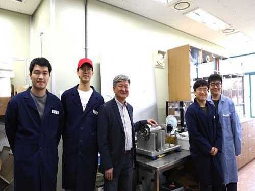
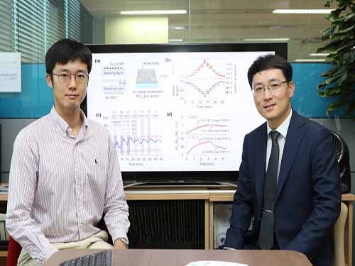
 KAIST Develops VRFB with Longer Durability
(from left: PhD candidate Soohyun Kim, Professor Hee-Tak Kim and PhD candidate Junghoon Choi)
There has been growing demand for large-scale storage for energy produced from renewable energy sources in an efficient and stable way. To meet this demand, a KAIST research team developed a new vanadium redox-flow battery (VRFB) with 15 times greater capacity retention and five times longer durability. This VRFB battery can be an excellent candidate for a large-scale rechargeable battery with no risk of explosion.
The VRFB has received much attention for its high efficiency and reliability with the absence of cross-contamination. However, it has the limitation of having insufficient charge and discharge efficiency and a low capacity retention rate because its perfluorinated membrane is very permeable to any active materials. To minimize energy loss, it needs a membrane that has low vanadium ion permeability and high ion conductivity. Hence, there was an attempt to incorporate a hydrocarbon membrane that has low cost and high ion selectivity but it turned out that the VO₂+ caused chemical degradation, which led to shortening the battery life drastically.
To develop a membrane with pore sizes smaller than the hydrated size of vanadium ions yet larger than that of the protons, a research team co-led by Professor Hee-Tae Jung and Professor Hee-Tak Kim from the Department of Chemical and Biomolecular Engineering implemented a graphene-oxide framework (GOF) membrane by cross-linking graphene oxide nanosheets. They believed that GOF, having strong ion selectivity, would be a good candidate for the membrane component for the VRFB. The interlayer spacing between the GO sheets limited moisture expansion and provided selective ion permeation.
The GOF membrane increased the capacity retention of the VRFB, which showed a 15 times higher rate than that of perfluorinated membranes. Its cycling stability was also enhanced up to five times, compared to conventional hydrocarbon membranes.
These pore-sized-tuned graphene oxide frameworks will allow pore-sized tuning of membranes and will be applicable to electrochemical systems that utilize ions of various sizes, such as rechargeable batteries and sensors.
Professor Kim said, “Developing a membrane that prevents the mixing of positive and negative active materials has been a chronic issue in the field of redox-flow batteries. Through this research, we showed that nanotechnology can prevent this crossover issue and membrane degradation. I believe that this technology can be applied to various rechargeable batteries requiring large-scale storage.”
This research was published in Nano Letters on May 3.
Figure 1. Electrochemical performances of the VRFBs with Nafion 115, SPAES (sulfonated poly), and GOF/SPAES: discharge capacity
Figure 2. Schematic of the selective ion transfer of hydrated vanadium ions and protons in the GOF membrane and the molecular structure of the GOF membrane, showing that the GO nanosheets are cross-linked with EDA (ethylenediamine)
2018.09.20 View 8292
KAIST Develops VRFB with Longer Durability
(from left: PhD candidate Soohyun Kim, Professor Hee-Tak Kim and PhD candidate Junghoon Choi)
There has been growing demand for large-scale storage for energy produced from renewable energy sources in an efficient and stable way. To meet this demand, a KAIST research team developed a new vanadium redox-flow battery (VRFB) with 15 times greater capacity retention and five times longer durability. This VRFB battery can be an excellent candidate for a large-scale rechargeable battery with no risk of explosion.
The VRFB has received much attention for its high efficiency and reliability with the absence of cross-contamination. However, it has the limitation of having insufficient charge and discharge efficiency and a low capacity retention rate because its perfluorinated membrane is very permeable to any active materials. To minimize energy loss, it needs a membrane that has low vanadium ion permeability and high ion conductivity. Hence, there was an attempt to incorporate a hydrocarbon membrane that has low cost and high ion selectivity but it turned out that the VO₂+ caused chemical degradation, which led to shortening the battery life drastically.
To develop a membrane with pore sizes smaller than the hydrated size of vanadium ions yet larger than that of the protons, a research team co-led by Professor Hee-Tae Jung and Professor Hee-Tak Kim from the Department of Chemical and Biomolecular Engineering implemented a graphene-oxide framework (GOF) membrane by cross-linking graphene oxide nanosheets. They believed that GOF, having strong ion selectivity, would be a good candidate for the membrane component for the VRFB. The interlayer spacing between the GO sheets limited moisture expansion and provided selective ion permeation.
The GOF membrane increased the capacity retention of the VRFB, which showed a 15 times higher rate than that of perfluorinated membranes. Its cycling stability was also enhanced up to five times, compared to conventional hydrocarbon membranes.
These pore-sized-tuned graphene oxide frameworks will allow pore-sized tuning of membranes and will be applicable to electrochemical systems that utilize ions of various sizes, such as rechargeable batteries and sensors.
Professor Kim said, “Developing a membrane that prevents the mixing of positive and negative active materials has been a chronic issue in the field of redox-flow batteries. Through this research, we showed that nanotechnology can prevent this crossover issue and membrane degradation. I believe that this technology can be applied to various rechargeable batteries requiring large-scale storage.”
This research was published in Nano Letters on May 3.
Figure 1. Electrochemical performances of the VRFBs with Nafion 115, SPAES (sulfonated poly), and GOF/SPAES: discharge capacity
Figure 2. Schematic of the selective ion transfer of hydrated vanadium ions and protons in the GOF membrane and the molecular structure of the GOF membrane, showing that the GO nanosheets are cross-linked with EDA (ethylenediamine)
2018.09.20 View 8292 -
 Using Donut-shaped Lithium Sulfide for Higher Performing Batteries
(from left: Research Professor Fangmin Ye and Professor Hee-Tak Kim)
A KAIST research team developed a lithium-sulfur battery with a doughnut-shaped active material structure showing a record lifecycle of over 600 cycles. Having higher energy density and lower production cost than a lithium-ion battery (LIB), it can be used in electric vehicles that require a longer battery life.
There has been an intense research conducted for developing lithium-sulfur batteries with high energy density because LIBs only allow for a very short travel distance per charge. However, Li-S batteries are still unable to provide a longer lifecycle due to the poor reversibility of the lithium metal cathode.
To tackle this issue, Professor Hee-Tak Kim from the Department of Chemical and Biomolecular Engineering and his team used lithium sulfide (Li₂S) cathodes and combine them with graphite anodes to enhance energy density and lifecycles for the batteries.
Yet, lithium sulfide is costly and, so far, there has not been an electrode architecture and electrolyte design that enables a longer lifecycle between the graphite anodes and lithium sulfide cathodes.
Hence, the team produced a doughnut-shaped lithium sulfide cathode active material from low-cost lithium sulfide developed from raw materials. They have also developed a lithium sulfide ion battery with a graphite anode and lithium sulfide cathode using a high concentration salt electrolyte.
This doughnut-shaped lithium sulfide showed outstanding charge and discharge reversibility through improving the transfer of lithium ions. Its highly concentrated salt electrolyte formed a stable film on the surface of the graphite electrode, which showed strong durability.
Through this technology, the team achieved 30% higher energy density than that of conventional LIBs and secured a lifecycle of more than 600 cycles. This doughnut-shaped lithium sulfide-based electrode can be manufactured using low-cost raw materials and a single heat treatment process. The electrode can also be applied to existing LIBs.
Professor Kim said, “We have demonstrated that applying low-cost sulfur compounds to LIBs can improve both energy density and the lifecycle simultaneously.”
This research, led by Research Professor Fangmin Ye, was published in Advanced Science on May 7.
Figure 1. Structural characterization of Li₂SO₄/CNT and Li₂S/CNT electrodes and suggested mechanism for the formation of the holey-Li₂S nanoarchitecture
2018.09.19 View 6421
Using Donut-shaped Lithium Sulfide for Higher Performing Batteries
(from left: Research Professor Fangmin Ye and Professor Hee-Tak Kim)
A KAIST research team developed a lithium-sulfur battery with a doughnut-shaped active material structure showing a record lifecycle of over 600 cycles. Having higher energy density and lower production cost than a lithium-ion battery (LIB), it can be used in electric vehicles that require a longer battery life.
There has been an intense research conducted for developing lithium-sulfur batteries with high energy density because LIBs only allow for a very short travel distance per charge. However, Li-S batteries are still unable to provide a longer lifecycle due to the poor reversibility of the lithium metal cathode.
To tackle this issue, Professor Hee-Tak Kim from the Department of Chemical and Biomolecular Engineering and his team used lithium sulfide (Li₂S) cathodes and combine them with graphite anodes to enhance energy density and lifecycles for the batteries.
Yet, lithium sulfide is costly and, so far, there has not been an electrode architecture and electrolyte design that enables a longer lifecycle between the graphite anodes and lithium sulfide cathodes.
Hence, the team produced a doughnut-shaped lithium sulfide cathode active material from low-cost lithium sulfide developed from raw materials. They have also developed a lithium sulfide ion battery with a graphite anode and lithium sulfide cathode using a high concentration salt electrolyte.
This doughnut-shaped lithium sulfide showed outstanding charge and discharge reversibility through improving the transfer of lithium ions. Its highly concentrated salt electrolyte formed a stable film on the surface of the graphite electrode, which showed strong durability.
Through this technology, the team achieved 30% higher energy density than that of conventional LIBs and secured a lifecycle of more than 600 cycles. This doughnut-shaped lithium sulfide-based electrode can be manufactured using low-cost raw materials and a single heat treatment process. The electrode can also be applied to existing LIBs.
Professor Kim said, “We have demonstrated that applying low-cost sulfur compounds to LIBs can improve both energy density and the lifecycle simultaneously.”
This research, led by Research Professor Fangmin Ye, was published in Advanced Science on May 7.
Figure 1. Structural characterization of Li₂SO₄/CNT and Li₂S/CNT electrodes and suggested mechanism for the formation of the holey-Li₂S nanoarchitecture
2018.09.19 View 6421 -
 Transfering Nanowires onto a Flexible Substrate
(from left: PhD Min-Ho Seo and Professor Jun-Bo Yoon)
Boasting excellent physical and chemical properties, nanowires (NWs) are suitable for fabricating flexible electronics; therefore, technology to transfer well-aligned wires plays a crucial role in enhancing performance of the devices. A KAIST research team succeeded in developing NW-transfer technology that is expected to enhance the existing chemical reaction-based NW fabrication technology that has this far showed low performance in applicability and productivity.
NWs, one of the most well-known nanomaterials, have the structural advantage of being small and lightweight. Hence, NW-transfer technology has drawn attention because it can fabricate high-performance, flexible nanodevices with high simplicity and throughput.
A conventional nanowire-fabrication method generally has an irregularity issue since it mixes chemically synthesized nanowires in a solution and randomly distributes the NWs onto flexible substrates. Hence, numerous nanofabrication processes have emerged, and one of them is master-mold-based, which enables the fabrication of highly ordered NW arrays embedded onto substrates in a simple and cost-effective manner, but its employment is limited to only some materials because of its chemistry-based NW-transfer mechanism, which is complex and time consuming. For the successful transfer, it requires that adequate chemicals controlling the chemical interfacial adhesion between the master mold, NWs, and flexible substrate be present.
Here, Professor Jun-Bo Yoon and his team from the School of Electrical Engineering introduced a material-independent mechanical-interlocking-based nanowire-transfer (MINT) method to fabricate ultralong and fully aligned NWs on a large flexible substrate in a highly robust manner.
This method involves sequentially forming a nanosacrificial layer and NWs on a nanograting substrate that becomes the master mold for the transfer, then weakening the structure of the nanosacrificial layer through a dry etching process. The nanosacrificial layer very weakly holds the nanowires on the master mold. Therefore, when using a flexible substrate material, the nanowires are very easily transferred from the master mold to the substrate, just like a piece of tape lifting dust off a carpet.
This technology uses common physical vapor deposition and does not rely on NW materials, making it easy to fabricate NWs onto the flexible substrates.
Using this technology, the team was able to fabricate a variety of metal and metal-oxide NWs, including gold, platinum, and copper – all perfectly aligned on a flexible substrate. They also confirmed that it can be applied to creating stable and applicable devices in everyday life by successfully applying it to flexible heaters and gas sensors.
PhD Min-Ho Seo who led this research said, “We have successfully aligned various metals and semiconductor NWs with excellent physical properties onto flexible substrates and applied them to fabricated devices. As a platform-technology, it will contribute to developing high-performing and stable electronic devices.”
This research was published in ACS Nano on May 24.
Figure 1. Photograph of the fabricated wafer-scale fully aligned and ultralong Au nanowire array on a flexible substrate
2018.09.17 View 7032
Transfering Nanowires onto a Flexible Substrate
(from left: PhD Min-Ho Seo and Professor Jun-Bo Yoon)
Boasting excellent physical and chemical properties, nanowires (NWs) are suitable for fabricating flexible electronics; therefore, technology to transfer well-aligned wires plays a crucial role in enhancing performance of the devices. A KAIST research team succeeded in developing NW-transfer technology that is expected to enhance the existing chemical reaction-based NW fabrication technology that has this far showed low performance in applicability and productivity.
NWs, one of the most well-known nanomaterials, have the structural advantage of being small and lightweight. Hence, NW-transfer technology has drawn attention because it can fabricate high-performance, flexible nanodevices with high simplicity and throughput.
A conventional nanowire-fabrication method generally has an irregularity issue since it mixes chemically synthesized nanowires in a solution and randomly distributes the NWs onto flexible substrates. Hence, numerous nanofabrication processes have emerged, and one of them is master-mold-based, which enables the fabrication of highly ordered NW arrays embedded onto substrates in a simple and cost-effective manner, but its employment is limited to only some materials because of its chemistry-based NW-transfer mechanism, which is complex and time consuming. For the successful transfer, it requires that adequate chemicals controlling the chemical interfacial adhesion between the master mold, NWs, and flexible substrate be present.
Here, Professor Jun-Bo Yoon and his team from the School of Electrical Engineering introduced a material-independent mechanical-interlocking-based nanowire-transfer (MINT) method to fabricate ultralong and fully aligned NWs on a large flexible substrate in a highly robust manner.
This method involves sequentially forming a nanosacrificial layer and NWs on a nanograting substrate that becomes the master mold for the transfer, then weakening the structure of the nanosacrificial layer through a dry etching process. The nanosacrificial layer very weakly holds the nanowires on the master mold. Therefore, when using a flexible substrate material, the nanowires are very easily transferred from the master mold to the substrate, just like a piece of tape lifting dust off a carpet.
This technology uses common physical vapor deposition and does not rely on NW materials, making it easy to fabricate NWs onto the flexible substrates.
Using this technology, the team was able to fabricate a variety of metal and metal-oxide NWs, including gold, platinum, and copper – all perfectly aligned on a flexible substrate. They also confirmed that it can be applied to creating stable and applicable devices in everyday life by successfully applying it to flexible heaters and gas sensors.
PhD Min-Ho Seo who led this research said, “We have successfully aligned various metals and semiconductor NWs with excellent physical properties onto flexible substrates and applied them to fabricated devices. As a platform-technology, it will contribute to developing high-performing and stable electronic devices.”
This research was published in ACS Nano on May 24.
Figure 1. Photograph of the fabricated wafer-scale fully aligned and ultralong Au nanowire array on a flexible substrate
2018.09.17 View 7032