Electrical+Engineering
-
 New Technology Will Enable the Commercialization of Plasmon Displays
-- Enhancements in the penetration ratios of color filters are expected by applying nano-surface plasmon effects. --
-- Color filter technology will be applicable to large-area OLED and LCD. --
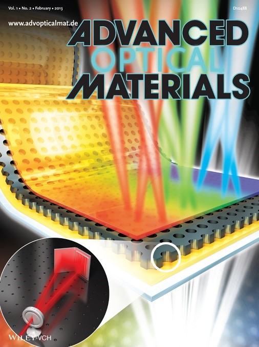
The fabrication technology to commercialize display color filters using plasmon effects has been discovered.
A joint research team headed by Professor Kyung Cheol Choi from the Department of Electrical Engineering of the Korea Advanced Institute for Science and Technology and Prof. Byeong-Kwon Ju from the School of Electrical Engineering of Korea University has developed the technology to design and produce a display color filter by applying nano-surface plasmon effects.
Color filters are core components used to express colors in CMOS image sensors found in LCD/OLED displays or digital cameras. The current color filters have penetration ratios of 20~30%, but the objective of the joint research team is to raise this penetration ratio by over 40% to facilitate the mass production of energy-efficient plasmonic displays.
Currently available plasmonic color filters are limited to applications on micrometer scales. However, outcomes of the newest research extend the size of the applications up to 2.5 cm by using laser interference lithography. The academic and industrial sectors agree that it is now possible to mass-produce displays using plasmonic color filters.
The researchers built a nanohole array to large scale by using laser interference lithography, a technology that forms nanostructures with laser light interferences. They also suggested a new manufacturing process that can optimize the features of color filters while compensating for defects arising from the fabrication stages.
The new manufacturing process of applying laser interference lithography is expected to overcome the shortcomings of traditional color filters by simplifying production and, enabling them to be produced at lower costs.
“There were limitations to industrial applications of plasmon effect due to production costs, time, and yields,” explained Yun Seon Do, a Ph. D. candidate in the Department of Electrical Engineering of KAIST. “The new technology can reduce fabrication time and cost to the extent that it would be advisable to replace dye-based and pigment-based color filter technology."
“This research can be applied to large-scale displays, such as TV screens, by using laser-interference lithography,” said Jung-Ho Park, a Ph. D. candidate in the School of Electrical Engineering of Korea University. “The research outcome is expected to be widely applied in advanced nano-manufacturing processes as it does not restrict the types of circuit boards."
The research outcome, led by doctoral candidates Do and Park, appeared on the front cover of the second issue of Advanced Optical Materials, a highly regarded academic journal in the field of nanotechnologies, and the team has applied for six related patents.
2013.03.13 View 10407
New Technology Will Enable the Commercialization of Plasmon Displays
-- Enhancements in the penetration ratios of color filters are expected by applying nano-surface plasmon effects. --
-- Color filter technology will be applicable to large-area OLED and LCD. --
The fabrication technology to commercialize display color filters using plasmon effects has been discovered.
A joint research team headed by Professor Kyung Cheol Choi from the Department of Electrical Engineering of the Korea Advanced Institute for Science and Technology and Prof. Byeong-Kwon Ju from the School of Electrical Engineering of Korea University has developed the technology to design and produce a display color filter by applying nano-surface plasmon effects.
Color filters are core components used to express colors in CMOS image sensors found in LCD/OLED displays or digital cameras. The current color filters have penetration ratios of 20~30%, but the objective of the joint research team is to raise this penetration ratio by over 40% to facilitate the mass production of energy-efficient plasmonic displays.
Currently available plasmonic color filters are limited to applications on micrometer scales. However, outcomes of the newest research extend the size of the applications up to 2.5 cm by using laser interference lithography. The academic and industrial sectors agree that it is now possible to mass-produce displays using plasmonic color filters.
The researchers built a nanohole array to large scale by using laser interference lithography, a technology that forms nanostructures with laser light interferences. They also suggested a new manufacturing process that can optimize the features of color filters while compensating for defects arising from the fabrication stages.
The new manufacturing process of applying laser interference lithography is expected to overcome the shortcomings of traditional color filters by simplifying production and, enabling them to be produced at lower costs.
“There were limitations to industrial applications of plasmon effect due to production costs, time, and yields,” explained Yun Seon Do, a Ph. D. candidate in the Department of Electrical Engineering of KAIST. “The new technology can reduce fabrication time and cost to the extent that it would be advisable to replace dye-based and pigment-based color filter technology."
“This research can be applied to large-scale displays, such as TV screens, by using laser-interference lithography,” said Jung-Ho Park, a Ph. D. candidate in the School of Electrical Engineering of Korea University. “The research outcome is expected to be widely applied in advanced nano-manufacturing processes as it does not restrict the types of circuit boards."
The research outcome, led by doctoral candidates Do and Park, appeared on the front cover of the second issue of Advanced Optical Materials, a highly regarded academic journal in the field of nanotechnologies, and the team has applied for six related patents.
2013.03.13 View 10407 -
 Inexpensive Separation Method of Graphene Developed
The problem with commercializing graphene that is synthesized onto metals over a wide area is that it can not be separated from the metal. However, a groundbreaking separation technology which is both cheap and environment friendly has been developed.
Prof. Taek soo Kim and Prof. Byung Jin Cho"s research teams have conducted this research under the support of the Global Frontier program and Researcher Support Program initiated by The Ministry of Education and Science and Korea Research Foundation. The research results have been posted on the online news flash of Nano Letters on februrary 29th. (Thesis title: Direct Measurement of Adhesion Energy of Monolayer Graphene As-Grown on Copper and Its Application to Renewable Transfer Process)
The research has generated exact results on the interfacial adhesive energy of graphene and its surface material for the first time. Through this, the catalyst metal are no longer to be used just once, but will be used for an infinite number of times, thereby being ecofriendly and efficient.
Wide area graphine synthesized onto the catalyst meatal are used in various ways such as for display and for solar cells. There has been much research going on in this field. However, in order to use this wide area graphene, the graphene must be removed from the catalyst metal without damage.
Until now, the metal had been melted away through the use of chemical substances in order to separate the graphene. However, this method has been very problematic. The metal can not be reused, the costs are very high, much harmful wastes were created in the process of melting the metals, and the process was very complicated.
The research teams of Professors Taek Su Kim and Byung Jin Cho measured the interfacial adhesive energy of the synthesized graphene and learned that it could be easily removed.
Also, the mechanically removed graphene was successfully used in creating molecular electronic devices directly. This has thus innovatively shortened the graphene manufacturing process. Also, it has been confirmed that the metalic board can be reused multiple times after the graphene is removed. A new, ecofriendly and cost friendly method of graphene manufacturing has been paved.
Through this discovery, it is expected that graphene will become easier to manufacture and that the period til the commercialization date of graphene will therefore be greatly reduced
Prof. Cho stated " This reserach has much academical meaning significance in that it has successfully defined the surfacial adhesive energy between the graphene and its catalyst material and it should receive much attention in that it solved the largest technical problem involved in the production of graphene.
2012.04.04 View 17075
Inexpensive Separation Method of Graphene Developed
The problem with commercializing graphene that is synthesized onto metals over a wide area is that it can not be separated from the metal. However, a groundbreaking separation technology which is both cheap and environment friendly has been developed.
Prof. Taek soo Kim and Prof. Byung Jin Cho"s research teams have conducted this research under the support of the Global Frontier program and Researcher Support Program initiated by The Ministry of Education and Science and Korea Research Foundation. The research results have been posted on the online news flash of Nano Letters on februrary 29th. (Thesis title: Direct Measurement of Adhesion Energy of Monolayer Graphene As-Grown on Copper and Its Application to Renewable Transfer Process)
The research has generated exact results on the interfacial adhesive energy of graphene and its surface material for the first time. Through this, the catalyst metal are no longer to be used just once, but will be used for an infinite number of times, thereby being ecofriendly and efficient.
Wide area graphine synthesized onto the catalyst meatal are used in various ways such as for display and for solar cells. There has been much research going on in this field. However, in order to use this wide area graphene, the graphene must be removed from the catalyst metal without damage.
Until now, the metal had been melted away through the use of chemical substances in order to separate the graphene. However, this method has been very problematic. The metal can not be reused, the costs are very high, much harmful wastes were created in the process of melting the metals, and the process was very complicated.
The research teams of Professors Taek Su Kim and Byung Jin Cho measured the interfacial adhesive energy of the synthesized graphene and learned that it could be easily removed.
Also, the mechanically removed graphene was successfully used in creating molecular electronic devices directly. This has thus innovatively shortened the graphene manufacturing process. Also, it has been confirmed that the metalic board can be reused multiple times after the graphene is removed. A new, ecofriendly and cost friendly method of graphene manufacturing has been paved.
Through this discovery, it is expected that graphene will become easier to manufacture and that the period til the commercialization date of graphene will therefore be greatly reduced
Prof. Cho stated " This reserach has much academical meaning significance in that it has successfully defined the surfacial adhesive energy between the graphene and its catalyst material and it should receive much attention in that it solved the largest technical problem involved in the production of graphene.
2012.04.04 View 17075 -
 Wireless electric trams at Seoul Amusement Park begin full operations.
Photo by Hyung-Joon Jun
IMMEDIATE RELEASE
Wireless electric trams at Seoul Amusement Park begin full operations.
KAIST’s On-Line Electric Vehicle (OLEV) becomes an icon of green technology, particularly for young students who aspire to transform their nation into the “vanguard of sustainability.”
Seoul, South Korea, July 19, 2011—As young students wrap up their school work before summer vacation in late July, Seoul Grand Park, an amusement park located south of Seoul, is busily preparing to accommodate throngs of summer visitors. Among the park’s routine preparations, however, there is something new to introduce to guests this summer: three wireless electric trams have replaced the old diesel-powered carts used by passengers for transportation within the park.
The Korea Advanced Institute of Science and Technology (KAIST) and the city of Seoul held a ceremony this morning, July 19, 2011, to celebrate their joint efforts to adopt a green public transportation system and presented park visitors with the three On-Line Electric Vehicles (OLEVs), which will be operated immediately thereafter. Approximately one hundred people, including science high school students across the nation, attended the ceremony and had a chance to ride the trams.
KAIST unveiled the prototype of an electric tram to the public in March 2010, and since then it has developed three commercial trams. The Korean government and the institute have worked on legal issues to embark on the full-scale commercialization of OLEV, and the long awaited approval from the government on such issues as standardization of the OLEV technology and road infrastructure, regulation of electromagnetic fields and electricity safety, and license and permits for vehicle eligibility, finally came through.
The On-Line Electric Vehicle (OLEV) is no ordinary electric car in that it is remotely charged via electromagnetic fields created by electric cables buried beneath the road. Unlike other currently available electric cars, OLEV can travel unlimited distances without having to stop to recharge. OLEV also has a small battery onboard, which enables the vehicle to travel on roads that are not equipped with underground power cables. This battery, however, is only one-fifth of the size of a conventional electric vehicle battery, resulting in considerable savings in the cost, size, and weight of the vehicle.
The OLEV project was initiated in 2009 as a method of resolving the battery problems of electric cars in a creative and disruptive way. KAIST came up with the idea of supplying electricity directly to the cars instead of depending solely on the onboard battery for power. Since then, the university has developed core technologies related to OLEV such as the “Shaped Magnetic Field in Resonance (SMFIR),” which enables an electric car to collect the magnetic fields and convert them into electricity, and the “Segment Technology,” which controls the flow of electromagnetic waves through an automatic power-on/shut-down system, thereby eliminating accidental exposure of the electromagnetic waves to pedestrians or non-OLEV cars.
According to KAIST, three types of OLEV have been developed thus far: electric buses, trams, and sport utility vehicles (SUVs). The technical specifications of the most recently developed OLEV (an electric bus), the OLEV research team at the university said, are as follows:
· Power cables are buried 15cm beneath the road surface.
· On average, over 80% power transmission efficiency is achieved.
· The distance gap between the road surface and the underbody of the vehicle is 20cm.
· The OLEV bus has a maximum electricity pickup capacity of 100kW.
· The OLEV bus complies with international standards for electromagnetic fields (below 24.1 mG).
The eco-friendly electric trams at Seoul Grand Park consume no fossil fuels and do not require any overhead wires or cables. Out of the total circular driving route (2.2km), only 16% of the road, 372.5m, has the embedded power lines, indicating that OLEV does not require extensive reconstruction of the road infrastructure. The city government of Seoul signed a memorandum of understanding with KAIST in 2009 as part of its initiatives to curtail emissions from public transportation and provide cleaner air to its citizens. Both parties plan to expand such collaboration to other transportation systems including buses in the future.
KAIST expects the OLEV technology to be applied in industries ranging from transportation to electronics, aviation, maritime transportation, robotics, and leisure. There are several ongoing international collaborative projects to utilize the OLEV technology for a variety of transportation needs, such as inner city commute systems (bus and trolley) and airport shuttle buses, in nations including Malaysia, US, Germany, and Denmark.
# # #
More information about KAIST’s On-Line Electric Vehicle can be found at http://olev.co.kr/en/index.php. For any inquiries, please contact Lan Yoon at 82-42-350-2295 (cell: 82-10-2539-4303) or by email at hlyoon@kaist.ac.kr.
2011.07.22 View 17257
Wireless electric trams at Seoul Amusement Park begin full operations.
Photo by Hyung-Joon Jun
IMMEDIATE RELEASE
Wireless electric trams at Seoul Amusement Park begin full operations.
KAIST’s On-Line Electric Vehicle (OLEV) becomes an icon of green technology, particularly for young students who aspire to transform their nation into the “vanguard of sustainability.”
Seoul, South Korea, July 19, 2011—As young students wrap up their school work before summer vacation in late July, Seoul Grand Park, an amusement park located south of Seoul, is busily preparing to accommodate throngs of summer visitors. Among the park’s routine preparations, however, there is something new to introduce to guests this summer: three wireless electric trams have replaced the old diesel-powered carts used by passengers for transportation within the park.
The Korea Advanced Institute of Science and Technology (KAIST) and the city of Seoul held a ceremony this morning, July 19, 2011, to celebrate their joint efforts to adopt a green public transportation system and presented park visitors with the three On-Line Electric Vehicles (OLEVs), which will be operated immediately thereafter. Approximately one hundred people, including science high school students across the nation, attended the ceremony and had a chance to ride the trams.
KAIST unveiled the prototype of an electric tram to the public in March 2010, and since then it has developed three commercial trams. The Korean government and the institute have worked on legal issues to embark on the full-scale commercialization of OLEV, and the long awaited approval from the government on such issues as standardization of the OLEV technology and road infrastructure, regulation of electromagnetic fields and electricity safety, and license and permits for vehicle eligibility, finally came through.
The On-Line Electric Vehicle (OLEV) is no ordinary electric car in that it is remotely charged via electromagnetic fields created by electric cables buried beneath the road. Unlike other currently available electric cars, OLEV can travel unlimited distances without having to stop to recharge. OLEV also has a small battery onboard, which enables the vehicle to travel on roads that are not equipped with underground power cables. This battery, however, is only one-fifth of the size of a conventional electric vehicle battery, resulting in considerable savings in the cost, size, and weight of the vehicle.
The OLEV project was initiated in 2009 as a method of resolving the battery problems of electric cars in a creative and disruptive way. KAIST came up with the idea of supplying electricity directly to the cars instead of depending solely on the onboard battery for power. Since then, the university has developed core technologies related to OLEV such as the “Shaped Magnetic Field in Resonance (SMFIR),” which enables an electric car to collect the magnetic fields and convert them into electricity, and the “Segment Technology,” which controls the flow of electromagnetic waves through an automatic power-on/shut-down system, thereby eliminating accidental exposure of the electromagnetic waves to pedestrians or non-OLEV cars.
According to KAIST, three types of OLEV have been developed thus far: electric buses, trams, and sport utility vehicles (SUVs). The technical specifications of the most recently developed OLEV (an electric bus), the OLEV research team at the university said, are as follows:
· Power cables are buried 15cm beneath the road surface.
· On average, over 80% power transmission efficiency is achieved.
· The distance gap between the road surface and the underbody of the vehicle is 20cm.
· The OLEV bus has a maximum electricity pickup capacity of 100kW.
· The OLEV bus complies with international standards for electromagnetic fields (below 24.1 mG).
The eco-friendly electric trams at Seoul Grand Park consume no fossil fuels and do not require any overhead wires or cables. Out of the total circular driving route (2.2km), only 16% of the road, 372.5m, has the embedded power lines, indicating that OLEV does not require extensive reconstruction of the road infrastructure. The city government of Seoul signed a memorandum of understanding with KAIST in 2009 as part of its initiatives to curtail emissions from public transportation and provide cleaner air to its citizens. Both parties plan to expand such collaboration to other transportation systems including buses in the future.
KAIST expects the OLEV technology to be applied in industries ranging from transportation to electronics, aviation, maritime transportation, robotics, and leisure. There are several ongoing international collaborative projects to utilize the OLEV technology for a variety of transportation needs, such as inner city commute systems (bus and trolley) and airport shuttle buses, in nations including Malaysia, US, Germany, and Denmark.
# # #
More information about KAIST’s On-Line Electric Vehicle can be found at http://olev.co.kr/en/index.php. For any inquiries, please contact Lan Yoon at 82-42-350-2295 (cell: 82-10-2539-4303) or by email at hlyoon@kaist.ac.kr.
2011.07.22 View 17257